What Is a Monolithic Ceramic Capacitor?
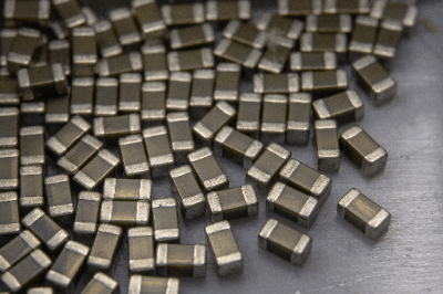 A monolithic ceramic capacitor, also called MLCC (Multi-Layer Ceramic Capacitor), is a chip component type capacitor with multiple layers of internal electrodes and dielectric layers. Further evolution is expected in the capacitor industry, where miniaturization and capacitance increase.
Barium titanate and titanium oxide are mainly used as dielectric, and the inner electrode and dielectric are formed in multiple layers. Increasing the number of layers makes it possible to increase the capacitance, leading to miniaturization of MLCCs.
Recently, the mainstream sizes of MLCCs are 0603 (0.6×0.3mm) and 0402 (0.4×0.2mm). The next generation 0201 size has already been realized in some capacitance values, but it has not yet become widespread in the market due to handling difficulties.
Monolithic ceramic capacitors are available in chip and radial types. Compared to other capacitors, multilayer ceramic capacitors have low high-frequency impedance and ESR (equivalent series resistance) and good high-frequency characteristics.
Types of Monolithic Ceramic Capacitors
Monolithic ceramic capacitors are available in a wide range of characteristics, and the size, withstand voltage, temperature characteristics, and other factors must be taken into consideration when determining the type of capacitor to be used for a particular application. Monolithic ceramic capacitors can be broadly classified into Class 1 and Class 2 in terms of their characteristics.
1. Class 1
Class 1 capacitors are also called temperature compensated capacitors, and can be compensated relatively easily because they have extremely low ESR, little temperature variation in capacitance, and the variation is linear.
However, the capacitance is usually small, ranging from 1pF to 1μF. ESRs are mainly used in applications where changes in capacitance are undesirable, such as oscillator circuits and time constant circuits.
2. Class 2
Class 2 is also called ferroelectric type, and its main material is barium titanate, which provides large capacitance of about 100 μF even in a small size. However, there are many points to keep in mind when using it, such as a large ESR, large temperature fluctuation of capacitance, and a decrease in actual capacitance when a DC bias is applied.
Therefore, when adopting Class 2 monolithic ceramic capacitors, it is essential to design circuits with their characteristics in mind. The main applications of Class 2 multilayer ceramic capacitors are in circuits where slight changes in capacitance have little effect, such as power source smoothing and decoupling capacitors.
Applications of Monolithic Ceramic Capacitors
Monolithic ceramic capacitors have a wide range of applications because their performance can be selected according to the number of layers and their lineup is broad. Monolithic ceramic capacitors are used in cellular phones, televisions, and industrial equipment for decoupling, coupling, and smoothing circuits, in DC/DC converters, in computer power supplies, and for noise reduction.
For automotive applications, long-life and failure-resistant products are selected. For industrial equipment, high capacitance and small capacitors are widely used, and in recent years they have been replacing other capacitors.
Currently, the mainstream monolithic ceramic cCapacitors are quite small, with sizes of 1005 (1.0 x 0.5 x 0.5 mm) and 0603 (0.6 x 0.3 x 0.3 mm), but in the future, ultra-small capacitors such as 0402 (already in use in the market) and 0201 (the next generation) are expected to become mainstream. However, it is expected that ultra-small capacitors such as the 0402 size, which is already in use in the market, and the next-generation 0201 size will become mainstream.
Principle of Monolithic Ceramic Capacitor
The capacitance C of a capacitor is proportional to the dielectric constant ε and the electrode area S, and inversely proportional to the distance d between electrodes. When capacitors are connected in parallel, the overall capacitance is equal to the sum of the capacitances of each capacitor.
Therefore, the key to increasing the capacitance of a capacitor is to use a dielectric with a high dielectric constant, increase the electrode area, and make the distance between electrode plates as small as possible. A monolithic ceramic capacitor has a structure of many layers of very thin electrode plates, which can be considered as many capacitors with close distance between electrode plates connected in parallel.
In other words, the number of layers N is proportional to the capacitance C of the capacitor. Therefore, by increasing the capacitance with the number of layers N, monolithic ceramic capacitors can be made both smaller and larger.
Although barium titanate, which has a very high dielectric constant, is used as a dielectric in most cases, its performance is expected to eventually reach a plateau. Therefore, the development of materials with a superior dielectric constant and less susceptible to wear and tear is expected.
Structure of Monolithic Ceramic Capacitors
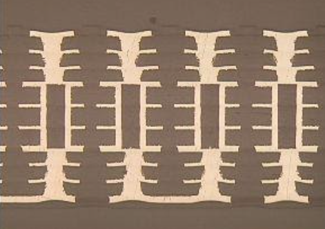
Nickel is used for the electrodes and barium titanate is mainly used for the dielectric. Nickel paste, which serves as the internal electrode, is applied to the dielectric in the form of a sheet, and the sheet is then layered and formed under pressure.
It is then cut into small pieces and sintered at about 1000°C. When the external electrodes are attached, the capacitor becomes a monolithic ceramic capacitor. By ensuring that the internal electrodes are connected to the external electrodes alternately on the left and right, the layers are in the same state as if they were joined in parallel.
Since they are produced in sheet form, they have become more efficient, smaller, and thinner. The number of layers can be as many as 1,000. The dielectric materials are classified into two types: low dielectric constant type, which mainly uses titanium oxide, and high dielectric constant type, which uses barium titanate.
Class 1 is used for temperature compensation and low capacitance in signal circuits, etc. Class 2 has a high dielectric constant and a large temperature coefficient, and is used for power supply decoupling and smoothing circuits.
Other Information on Monolithic Ceramic Capacitors
1. Characteristics of Monolithic Ceramic Capacitors
Monolithic ceramic capacitors have a capacitance that varies with temperature. Therefore, when selecting a monolithic ceramic capacitor, you should not only select one based on its capacitance and voltage rating, but also consider the temperature in the operating environment.
Monolithic ceramic capacitors are characterized by low equivalent series resistance (ESR) due to the use of metals such as nickel and copper in the electrodes. Monolithic ceramic capacitors also feature low parasitic inductance (ESL) due to their structure, which makes them suitable for use at high frequencies.
By taking advantage of these features of low ESR and ESL, it is possible to form resonant circuits with high Q-values and low-loss matching circuits, making MLCCs an indispensable component in the field of high-frequency circuit products, as well as in power supply decoupling and noise suppression applications.
By changing the number of layers of electrode plates, it is possible to control the capacitance from small to large. Therefore, a monolithic ceramic capacitor as a product is also characterized by a very wide range of capacitance in the prepared lineup.
2. Basic Technology for Large Capacitance
The capacitance of a capacitor increases in proportion to the area of the internal electrode plates. To achieve high capacitance without changing the size of the monolithic ceramic capacitor, it is important to stack as many electrode layers as possible.
In general, in order to achieve miniaturization and high capacitance, it is necessary to stack electrodes with sub-millimeter order thickness, so thinning electrode layers is an essential technology. For thinning the electrode layer, adjustment of barium oxide, the raw material of dielectric, and printing technology for forming the internal electrode in paste form into a sheet are important.
The dielectric is made of fine particles called grain, which are formed by adding additives to barium oxide, printing it in sheet form, and then sintering it. How the microstructure of the grains is designed is critical to ensure that the thin-layer dielectric functions adequately.
Screen printing technology, such as that used for silk screens, is used to print thin internal electrodes on the paste. By extruding the paste through the micropores, it is possible to form a uniform thin layer of internal electrode.
3. Share of Monolithic Ceramic Capacitors
Monolithic ceramic capacitors are so widely used in the world of electronics that they are now considered the rice of industry. For example, about 200 to 300 monolithic ceramic capacitors are used per TV receiver, and about 1,000 monolithic ceramic capacitors are used per smartphone.
Electric vehicles use more than 15,000 capacitors per vehicle. Japanese companies account for a large share of the production of these multilayer ceramic capacitors. Although the data is a bit old, the top four companies in terms of market share by value in 2017 are as follows, with three Japanese companies accounting for the majority of the global market share.
- Murata: 33.9% (will exceed 40% in 2020)
- Samsung Electro-Mechanics: 18.1
- Taiyo Yuden: 10.3
- TDK: 8.4
High-performance monolithic ceramic capacitors are especially demanded in automobiles, and Murata and TDK dominate the global market. Monolithic ceramic capacitors are expected to be in short supply for the time being, as their use is expected to further increase after 2021, when 5G generation smartphones will be in widespread use.
 Heat shrinkable tubing is tubing that has been processed to shrink when heat is applied.
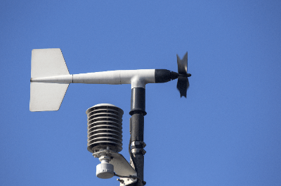 An anemometer is a device that measures the speed of the wind. Anemometers measure the speed of the wind and display it in units such as m/s or knots. Anemometers can be used to measure various wind speeds, such as those caused by atmospheric conditions, wind caused by rotation, and wind coming out of air conditioning exhaust vents.
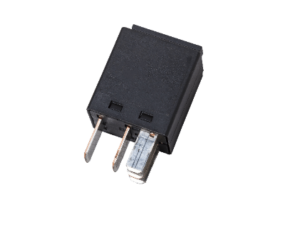 Power relays are relay components capable of carrying a current greater than 3A.