What Is a Build-Up Board?
A build-up board is a printed circuit board consisting of multiple layers.
The use of build-up substrates allows the use of high-density substrates in a small area, making it possible to create multifunctional products, even for small devices. Build-up substrates consist of layers of conductors and layers of insulators stacked on top of each other, with laser drilling and wire processing to penetrate the layers, making it possible to obtain complex substrates in a small area.
Emergence of Build-up Substrates
With the increasing density of substrates, it has become increasingly difficult to deal with the current via-hole structure alone. The development of cell phones has led to the demand for lighter, smaller, and more compact substrates, and substrates that can handle these demands have become necessary. Build-up boards began to appear around 2000 and have continued to the present day.
As the name “build-up” implies, it refers to a printed circuit board with many layers stacked on top of each other. Normally, a multilayer board can be built up into a single layer, but since it is built up many times, the number of processes increases, which means that it costs more. However, the use of this method is gaining momentum due to its ability to reduce wasted space and make small holes with a laser.
Reason 1: to reduce wasted space
When using via holes (holes to connect other layers) on a multilayer board, wiring cannot be done outside of the connecting layer because of the vias. Therefore, wiring efficiency will not be improved even if a multilayer board is used.
Reason 2: small holes can be drilled with a laser
Advances in equipment have made it possible to drill smaller holes at higher speeds with lasers than with drills. When drilling with a drill, the hole will penetrate the underlying layer. On the other hand, with lasers, it is possible to drill holes in the resin and stop the process on the copper, depending on the combination of conditions. Therefore, by repeating the process of drilling holes with a laser, plating, and then building up the next layer and processing it with a laser (build-up), the area of the via holes can be effectively used and high-density is possible.
By using build-up substrates, high-density substrates can be used in a small area, making it possible to create multifunctional products, even for small devices. Complex substrates in small areas can be obtained.
Uses of Build-up Substrates
Build-up substrates are widely used in small, lightweight electronic devices. When build-up substrates were first commercialized, they were used in PCs and cell phones. Today, they are used in small measurement devices, and IoT devices such as smart meters, digital camera modules, and PC peripherals.
The accuracy of drilling and other operations in the build-up board manufacturing process has a set standard, and it is necessary to choose exactly what level of accuracy to request when requesting the creation of a build-up board.
Build-up Substrate’s Process
This section describes the manufacturing process of build-up boards. The manufacturing process for build-up substrates includes insulator layer formation, via processing, smear removal, and plating on vias. Each of these processes is described below.
Formation of the Build-Up Layer
An insulator layer is built up on top of the printed circuit board. Prepreg, a rigid material, is used in some cases, while film is used in others. Prepreg is often used for digital cameras, smartphones, and semiconductor packages.
Via Processing
This is the process of drilling holes called vias in the insulator layer between substrates. Currently, holes are generally drilled using lasers.
Various types and wavelengths of lasers are used, including carbon dioxide gas and UV-YAG. Carbon dioxide lasers have a long wavelength (infrared) and are commonly used in digital cameras and smartphones, while UV-YAG lasers have a short wavelength (ultraviolet) and are used in high-density areas such as semiconductor package substrates.
Resin Residue Removal (Desmear)
The residue generated by laser processing is called smear. Resin residue cannot be connected, so it must be removed.
This process is called desmear. If the smear remains on the build-up substrate, it will lead to poor connections, etc., so it must be removed without fail. A strong chemical (potassium permanganate) must be used to remove the smear. However, recent high-speed resins may not be able to remove the smear by themselves, so plasma or other methods may be used in combination with the removal process.
Plating On Vias
Via plating is used to connect circuits between substrates with insulators in between. Since plating is done on small holes, it is necessary to prevent air bubbles from entering.
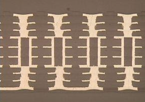
Names of Vias On Build-Up Boards
The names vary depending on the placement and structure of the holes, so a brief explanation is given below.
Staggered Vias
This is a method of shifting the position of vias like a staircase.
Stacked Vias
A via is stacked on top of another via. A via that overlaps on all layers is called a full-stack via.
Build-up Substrate Materials
Currently, two types of materials are mainstream: glass cloth, which is the same material used for ordinary substrates, and film, which is mainly used for packages. Looking at the past, various materials have been used, which are briefly explained below.
Originally, build-up substrates started when IBM developed a technology to support large computer flip-chip mounting for its product line. Various studies were conducted in the process.
As a result, we adopted a method of exposure and development using a UV-curing resin known as photovia. This had the advantage that vias could be formed in a batch. Since interlayer thickness was required, we developed and mass-produced the product based on solder materials resist for curtain coaters, which can earn film thickness. As with solder resist, an insulating layer was formed by applying, exposing, and developing, followed by final curing with heat.
After that, chemical copper is deposited and electrolytic copper plating is performed to form layer after layer. In addition, chemical copper formation is difficult to achieve peel strength because of the resin that causes photo-polymerization, and it is very difficult to control the conditions. In addition, the development process required a solvent and was subject to various regulations, so it could not be said to be a technology that would be widely used.
Subsequently, the micro via formation method was changed from optical formation to laser processing, as the processing speed of vias increased dozens of times due to the significant evolution of laser processing equipment. At that time, RCC (Resin Coated Copper Foil: copper foil with resin) was adopted. This is a thermosetting resin that is coated on top of the copper foil and is in the same semi-cured state as prepreg.
Therefore, it has the advantage that the lamination process, which is the same process used for conventional substrates, can be used. In addition, since peel strength is easy to achieve, via formation by light has been replaced by laser formation of RCC.
As electronic devices have become smaller and more handy, the use of build-up substrates has expanded. In this context, further cost reduction and reliability that can handle high density are required.
In addition, significant improvements in laser processing technology have made it possible to process commonly used materials with glass cloth, which has led to a significant shift to materials with glass cloth. Cell phones, digital cameras, and various types of mobiles are of this type.
On the other hand, in LSI packaging, high-density, multi-stage build-up has been demanded in response to higher-density LSI flip chips. To meet the demand for multiple layers and low thickness, thinner interlayer thickness, smaller vias, and flat surfaces are required. Film-type materials were developed to meet these requirements.
To fill the circuit with resin, a vacuum laminator is required, and a line dedicated to the unique process is needed to deposit chemical copper on the resin surface. This requires a large capital investment. In packaging applications, it is used for MPU large-scale LSI in PC smartphones.