What Is a Stepper?
A stepper is a projection exposure system used in photolithography, the manufacturing process of semiconductors and liquid crystals.
As IC circuit patterns become finer and finer, it has become more difficult to create photomask patterns of actual size, and a stepper is an exposure system that uses the step-and-repeat method to expose mask patterns larger than the actual size in a reduced projection exposure. The step-and-repeat method means that when exposing semiconductor wafers or LCD substrates, the exposure area is divided into several sections, and once one section is exposed, the exposure is moved to the next section (step) and repeated (repeat).
A stepper is a type of exposure system that exposes the entire area to be exposed while stepping and repeating.
Uses of Steppers
Steppers are used in the manufacture of semiconductors and liquid crystals, especially for exposure using masks in the photolithography process.
There are two types of stepper systems: the step-and-repeat system, which exposes wafers sequentially while stepping them because the area that can be transferred at one time is small; and the scanner system, which exposes wafers by scanning the reticle synchronously at a speed corresponding to the projection magnification. The latter is distinguished from steppers and is sometimes treated as a scanner.
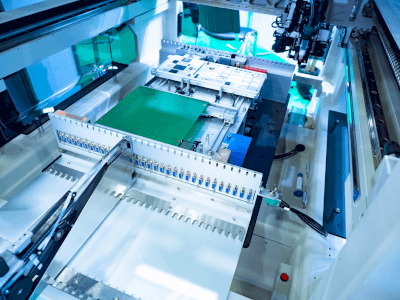
Principle of Steppers
Steppers uses a light source with a short wavelength to achieve high resolution in order to perform reduced projection exposures at high speed on large-diameter wafers and liquid crystals. The internal structure of steppers includes an exposure light source, projection lens, wafer stage, and wafer loader.
As the demand for large-scale integration of ICs increases, shorter wavelength exposure light sources are being used. In the 1990s, i-line light of 365nm was the principal light source. However, since then, shorter wavelengths such as Krf (wavelength: 248nm) and Arf (wavelength: 193nm) have been used.
A wafer stage is a stage that moves wafers at high speed in order to manufacture semiconductors such as ICs more quickly and with higher productivity. In addition to high-speed movement, high positioning accuracy is required for fine processing. The wafer loader is responsible for transporting wafers, such as removing wafers from the wafer stage and placing wafers on it.
Adhesion of foreign matter is a major enemy in IC manufacturing, and the sensitive wafers must be loaded and unloaded at high speed. Steppers are configured as shown above to perform sequential exposure while stepping wafers.
Other Information on Steppers
1. Immersion
Due to the high demand for precision, steppers and scanner systems, these days are equipped with large-scale mechanisms, and the price per unit is increasing. Therefore, as the wiring process nodes become finer, it is not desirable to suddenly make major changes to light sources and equipment mechanisms. There is a tendency to try to master the use of these devices by improving them over several generations.
One of the technologies to achieve this is “immersion.” Immersion refers to a method of increasing the exposure resolution of a light source by inserting a solution such as pure water between the resist on the wafer and the projection lens to shorten the wavelength of light compared to that in air. This is one of the technologies used in state-of-the-art photolithography processes.
2. EUV Lithography
Extreme ultraviolet lithography (EUV lithography) is the core of the next-generation exposure technology for the most advanced process nodes at a few nm, which can be exposed at a wavelength of 13.5nm, and is called extreme ultraviolet lithography. Although the world’s leading semiconductor manufacturers are using this technology to compete in cutting-edge processes, as of 2022, only one company in the world has commercialized EUV lithography equipment.