What Is a Pick and Place Machine?
A pick and place machine is a device and system designed to perform a series of operations: picking up an object in a specific position, transferring it to a predetermined position, unloading it, and placing it there.
In factories, pick-and-place can be said to be the mainstay of the line, regardless of the type of product. Pick-and-place systems can handle large objects that cannot be transported by human power, as well as small objects that require precise movement and installation on a micro scale.
Applications of Pick and Place Machines
Pick and place machines are used in the manufacturing process of many products, including automobiles, machine parts, electronic parts, electronic devices, home appliances, food, pharmaceuticals, cosmetics, paper, film, wire rod, construction materials, inspection, and testing. Although these systems are mainly used on factory production lines, they are also useful in the research field for the accurate movement, installation, and implantation of microscopic objects.
In addition, the system can improve on conventional problems such as time-consuming assembly due to the large number of parts, time-consuming adjustments, and too many complicated operation processes.
Principle of Pick and Place Machines
The implementation consists of a robot part that performs the operation, an arm part that executes the task, and a camera part that recognizes the target object. The process begins with the camera detecting the target object’s position. Based on image processing results, the robot moves to the target object’s location and utilizes the arm to pick it up.
Next, the robot moves to the designated placement area and gently releases the object. Pick methods can involve suction, suspension, or arm grasping. Pick-and-place systems are basically required to be more precise in terms of speed and accuracy, as they are related to productivity.
Flexibility, sensitivity, and strength are also required, depending on the nature of the work. The size of the machine itself is also designed so that it does not interfere with the production line and can be operated more easily.
Types of Pick and Place Machines
There are various types of pick and place machines, but the following are representative examples.
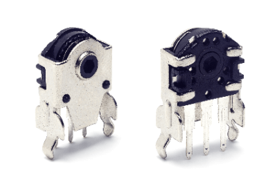
1. Cam System
The cam system uses a plate cam to convert the rotation of the input shaft into back-and-forth and up-and-down motion. The arm connects to linear slide guides, enabling both movements.
2. Roller Gear Cam System
The roller gear cam system consists of two sets of roller gear cams, one set of which converts rotational motion into forward/backward motion and the other set into up/down motion. Rotation of the input shaft allows the arm to move up, down, and up in sequence.
These mechanisms increase the speed of the pick and place machine by accelerating the rotation of the input shaft. Also, because positioning is done by cam, position repeatability is good, but strokes and other adjustments are not possible.
Speeds generally range from 0.2 to 0.5 seconds per cycle with a stroke of 100 mm or less, and position repeatability is about 0.02 mm.
Other Information on Pick and Place Machines
1. Pick-And-Place Robots
Some pick and place machines use articulated robots. Vertically articulated robots are not fast, but they are capable of various receiving and delivering postures, and large types can move heavy objects over a wide range.
SCARA robots are used for equipment such as automatic machines, where receiving and delivering are performed in a fixed posture and speed is required. SCARA robots can move horizontally at high speeds, enabling pick and place machine operations to be performed in about 0.4 seconds per cycle, which is about the same speed as a cam type robot. Some of them also have position repeatability of 0.01 mm or less, enabling high-speed, high-precision transfer.
Unlike the cam type, pick and place machines using an articulated robot can freely change the receiving and delivery positions and movement trajectory.
2. Control Method
Pick-and-place robots using articulated robots employ NC (numerical control) to manage precise robot movements, such as movement, rotation, and auxiliary movements of each axis.
G code describes the conditions and sequence of machining and movements such as positioning, while M code serves as a supplement to G code.
3. Advantages of Pick and Place Machines
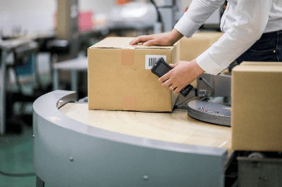
Pick and place machines are operations that require quick decision-making. They require instantaneous judgment of the shape and color of products flowing on the conveyor, tasks conventionally performed by hand.
Today, with the development of vision sensors and pick-and-place robots, accuracy and unwavering speed can be achieved. The pick-and-place robot does not suffer from the loss of speed caused by errors in judgment due to the loss of concentration that occurs with human hands.
In some workplaces, the physical and mental burden caused by the work being done with a person sitting in the middle of the back can also be eliminated.
 A handheld terminal is a portable terminal that can easily collect data recorded in barcodes and 2D codes.
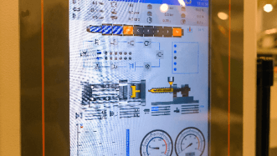 A programmable display is a display/operation device with a built-in computer that can be programmed.