What Is a Lead Frame?
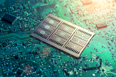
Lead frames are thin metal plates used within semiconductor device cases.
They are utilized in transistors, ICs, LSIs, photocouplers, LEDs, etc., with patterns designed to secure semiconductor devices, connect them to case terminals, and dissipate heat. Typically, copper or iron alloys are employed, with wiring patterns and external shapes created through press working and etching techniques.
Lead frames facilitate the high integration and functionality of semiconductor devices, utilizing metal materials renowned for their excellent electrical and thermal conductivity.
Applications of Lead Frames
1. Semiconductor Devices
Includes transistors, ICs, LSIs, photocouplers, LEDs, and diodes.
A photocoupler transmits electrical signals through light. A transistor, a semiconductor device, controls electrical signals, while a diode, also a semiconductor, allows current to flow in only one direction.
2. Electronic Components
Such as capacitors, resistors, and sensors.
3. Electrical Devices
Includes relays, motors, batteries, and switches.
4. Other
Pressure sensors, temperature sensors, actuators, and tact switches, the latter being a type of switch operated with a short stroke to produce instantaneous electrical signals.
Principle of Lead Frames
Lead frames ensure electrical and mechanical connections between semiconductor devices and the external environment. Comprised mainly of thin metal sheets with multiple electrodes, semiconductor elements are directly connected to these frames, facilitating the transmission of electrical connections to the outside.
They also play a vital role in dissipating the heat generated by semiconductor devices, thanks to their excellent thermal conductivity, ensuring the stable operation of these devices.
Properties of Lead Frames
1. Reliability
Lead frames significantly enhance the reliability of semiconductor devices. Precision in manufacturing is crucial for device reliability, necessitating stringent quality control to fulfill multiple functions. Their repeated use also underscores the importance of reliability.
2. Economical
Due to the ability to be mass-produced through stamping, lead frames are cost-effective. Technological advancements in surface treatment and processing have enabled high-precision manufacturing at reduced costs while maintaining reliability, making them prevalent in numerous electronic devices.
3. Conductivity
Primarily made from copper and iron alloys, lead frames boast exceptional electrical conductivity, crucial for the efficient transmission of electrical signals. Their conductive performance is further enhanced by plating.
4. Thermal Conductivity
Their material’s high thermal conductivity is vital for dissipating the heat from semiconductor devices efficiently. The large surface area of lead frames also facilitates heat dissipation through airflow.
5. Various Shapes
With the flexibility provided by stamping and etching techniques, lead frames can accommodate a wide range of shapes, allowing for diverse semiconductor device designs. This flexibility aids in enhancing device functionality and integration.
Etching, a technology for removing material surfaces chemically or physically, is essential for processing metal and semiconductor thin films.