What Is MOSFET?
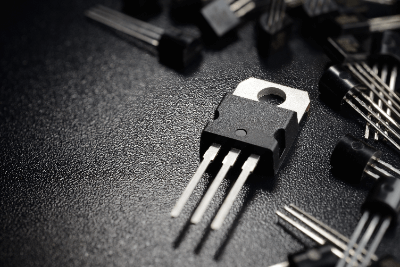 MOSFET is one of the semiconductor devices and a type of transistor that is indispensable in electronic devices.
MOS stands for “Metal Oxide Semiconductor” and FET stands for “Field-Effect Transistor.”
MOSFET performs on/off switching and signal amplification operations. One advantage is that they are very fast in operation and are suited for precise control.
Previously, semiconductor devices were dominated by high-polar transistors. However, with the increasing need for smaller, lighter, and more efficient devices, MOSFET has been becoming the mainstream semiconductor device in recent years.
Uses of MOSFET
MOSFETs are used as transistors in electronic circuit configurations for various ICs and LSIs.
Discrete applications include power electronics, sensors, and other industries, as well as power supply systems and inverters. Various LSIs are used in a wide range of applications, including microcontrollers for automobiles and information appliances, portable terminals such as smartphones and tablets, PC memory, and CPUs for various computers.
MOSFETs have become indispensable in recent products because they can be made smaller, lighter, and more integrated.
Principle of MOSFET
MOSFETs have three terminals (electrodes), called “drain,” “gate,” and “source,” respectively. By applying a voltage to the gate electrode, the MOSFET performs on/off switching and amplification operations as a transistor.
There are two types of MOSFET: N-channel (N-Ch) type and P-channel (P-Ch) type.
- N-channel (N-Ch) type
Current flows by applying a voltage to the gate that is more positive than the source potential. - P-channel (P-Ch) type
N-channel (N-Ch) type is often used because it is more convenient in terms of performance and circuitry.
CMOS (Complementary Metal-Oxide-Semiconductor), which is widely used in digital circuits, memory ICs, and sensors, consists of a pair of p-type and n-type MOS transistors. MOSFET has high operating speed and can switch at high speeds.
They are also suitable for high-frequency operation due to their low drive power. Although MOSFETs are not suitable for large currents, they have become a mainstay device in recent years due to their ease of integration and handling.
Types of MOSFET
MOSFET come in p-types and n-type types and are further classified into “enhancement type” and “depletion type” based on differences in operating characteristics.
1. Enhancement Type
Normal-off type, i.e., no current flows between source and drain when no voltage is applied to the gate.
2. Depletion Type
Normal-on type, i.e., current flows between source and drain even when no voltage is applied to the gate.
There are two types of MOSFET, but the enhancement type is the most commonly used for switching applications. The first MOSFET developed was the depletion type, but today it is used in very limited applications.
For example, assume a case where a negative power supply must be present in a circuit. When -5V is generated, the gate of the depletion type is connected here with a resistor of about 10kΩ.
Normally, if the negative voltage of -5V is output correctly, no current flows between the source and drain of the depletion type. However, if the negative power supply is not output correctly due to some abnormality, current flows between the source and drain, allowing an alert to be output.
How to Select MOSFET
The most important factor in selecting MOSFET is the absolute maximum rating of the source-to-drain withstand voltage VDSS. This is because the larger the withstand voltage of MOSFET, the higher its ON-resistance tends to be. If the optimum withstand voltage is not selected with a margin in consideration of the system application, ON-resistance will be unnecessarily high, leading to an increase in system power consumption.
If the voltage applied between source and drain is almost constant, the selection can be done without any problem, but the problem is how to take into account the case of a surge. If surge voltage is included, a margin of several times the steady-state rating must be considered.
Even MOSFETs with the same withstand voltage may have different withstand capacities for avalanche currents and avalanche energies. If you consider including surge energy, choose a MOSFET with high avalanche energy to obtain a MOSFET with lower breakdown voltage and lower ON-resistance.
Other Information on MOSFET
1. How Si-MOSFETs Are Different From IGBTs
Si-MOSFETs are not suitable for high-current applications. For power device applications such as high bias operation above 2V or inverter circuits for high current, IGBTs, which integrate MOSFET on the gate and a bipolar transistor on the output, are more suitable.
IGBTs are complex devices that generally require a gate driver circuit for operation, and are more difficult to handle than MOSFET because of their SOA (Safety Operation Area) and their tendency to break down when their absolute maximum ratings are exceeded, which requires a protection circuit.
Recently, SiC-MOSFETs, which use SiC, a compound semiconductor, instead of Si as the MOSFET substrate and have a larger band gap, have become popular because of their higher breakdown voltage characteristics. Since these devices have advantages and disadvantages, including cost, for the time being, they will be separated according to their applications in the market.
2. Information on SOI-CMOS
MOSFET has been improved in terms of ON-resistance and other characteristics through process miniaturization to support higher frequencies. In the past, CMOS structures with well layers were generally formed on p-type (or n-type) Si substrates called bulk substrates.
However, due to the need for high-frequency devices, especially for RF mobile applications, CMOS devices with improved high-frequency characteristics have emerged, in which the leakage path unique to MOSFET are suppressed by introducing an insulating BOX layer called SOI (Silicon On Insulator) instead of a bulk Si substrate to increase the substrate’s insulating property. CMOS devices with improved high-frequency characteristics are now available.
These devices are called SOI-CMOS and are attracting attention as devices with high-speed operation and low loss.
3. Process Miniaturization of MOSFET
The most important feature of MOSFETs are that they are semiconductor devices with low power consumption and suitable for large-scale integration. However, by making the process dimensions finer, it is possible to operate transistors at higher speeds and lower voltages and to dramatically increase the level of circuit integration.
In the case of the aforementioned CMOS-based large-scale digital processors, where integration is extremely important, the process size is said to be 3 nm as of 2022, compared to 100 nm in the early 2000s. The structure of the FinFET is based on a cutting-edge process that incorporates an ingenious transistor cross-section structure.
Although it is difficult to predict further miniaturization in the future, one technological trend that is being actively considered is the introduction of a three-dimensional chip mounting technology called a chiplet with a multi-chip structure, mainly by research and development organizations around the world.