What Is a Scanning Electron Microscope (SEM)?
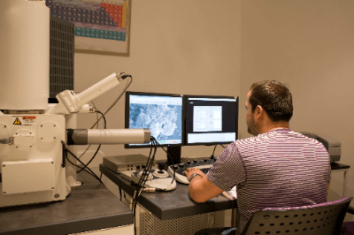
A SEM (scanning electron microscope) is a type of electron microscope that allows us to observe the surface conditions of a sample by irradiating the sample with electron beams and detecting the secondary electrons emitted from the sample.
A SEM makes it possible to observe even minute structures that are difficult to observe with an optical microscope. For this reason, it is used in a wide range of fields, such as materials engineering and biochemistry.
Uses of SEMs
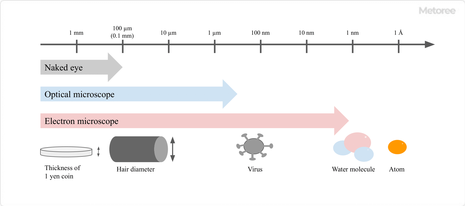
Figure 1. Types and resolutions of microscopes
The magnification of SEMs can be increased to several hundred thousand times, and the resolution can be increased to several nm. It also has features such as a deep depth of focus that make it easy to observe unevenness in the sample.
The magnification limit of an optical microscope is about 1,000x and the resolution limit is about 150nm.
In addition, unlike images obtained with optical microscopes, SEMs provide three-dimensional images with contrast, in which the plane perpendicular to the direction of incidence of the electron beam is darker and the closer the plane is to parallel, the brighter the image becomes.
Taking advantage of these features, SEMs are used to observe the surface conditions of various materials, such as semiconductor and ceramic materials, microorganisms such as bacteria and viruses, and biological samples such as cells. On the other hand, transmission electron microscopes are generally used to observe the internal structure of samples.
Principle of SEMs
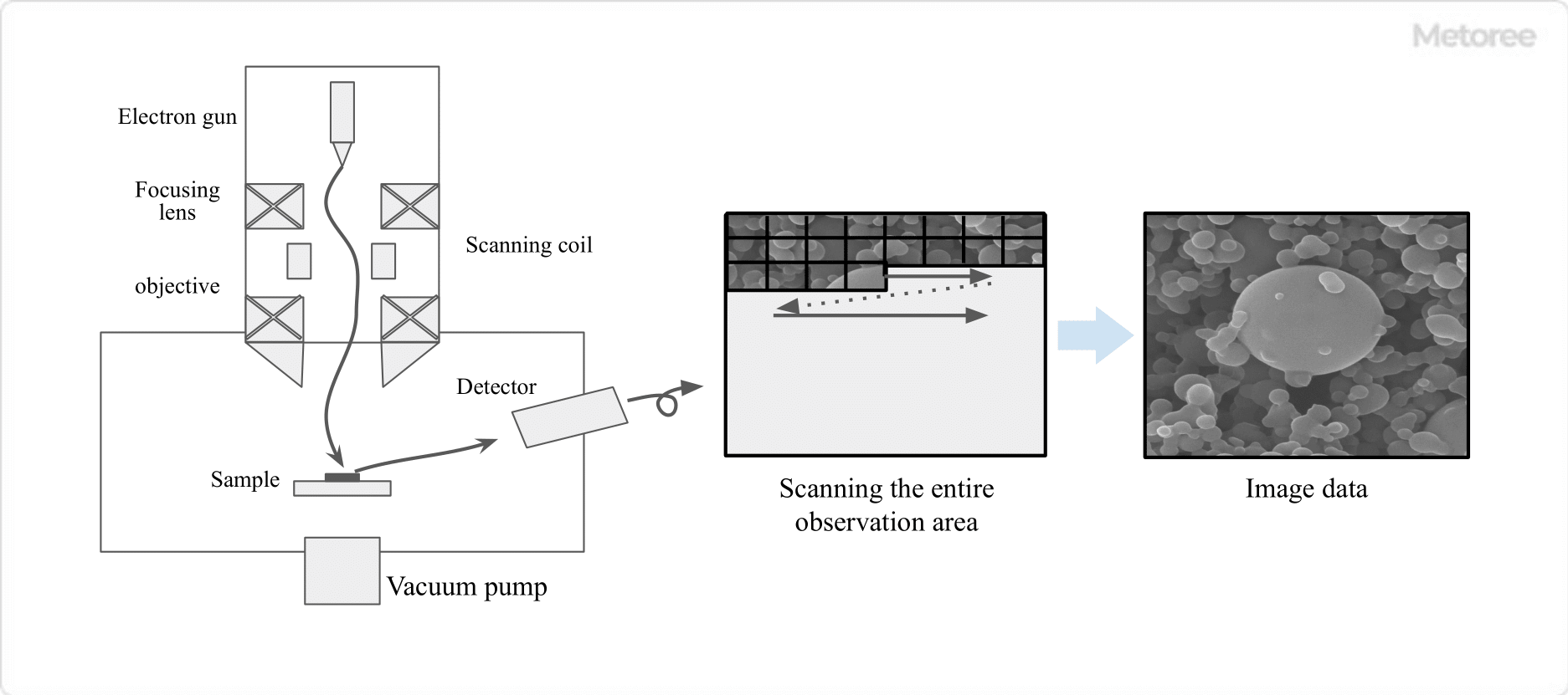
Figure 2. Structure and measurement image of scanning electron microscope
In SEMs, an accelerated electron beam is focused on the surface of a sample and irradiated, and the secondary electrons (SE) and backscattered electrons (BSE) generated during the irradiation are detected and analyzed.
By increasing the acceleration voltage and irradiating electron energy, the resolution can be increased to a few nm. Increasing the acceleration voltage increases the resolution. However, too high an acceleration voltage can cause problems such as the influence of reflected electrons from deeper positions in the sample and charging. Therefore, acceleration voltages of several kV to several tens of kV are usually used.
Secondary electrons are electrons ejected from near the surface of the sample when an electron beam is applied.
The state of the electrons differs according to the unevenness of the sample, creating contrast in the image data obtained by measuring secondary electrons and allowing observation of surface irregularities and particle shapes.
Backscattered electrons, on the other hand, are electrons that are bounced back when an electron beam interacts with an atom.
The reflectance of the emitted electrons differs depending on the atom. By measuring backscattered electrons, the contrast is enhanced for each type of atom and the distribution of atoms in the sample can be observed.
Structure of SEMs
SEMs mainly consist of an electron gun that emits electron beams, an electron lens that focuses the electron beams onto the sample surface, and a detector that detects secondary electrons and backscattered electrons.
There are three types of electron guns: thermal electron emission, field emission, and Schottky type, each with different characteristics. Electron lenses are generally of the type in which an electric current is passed through a coil and the electron beam is controlled by a magnetic field, and there are various types, such as the out-lens type and in-lens type.
The inside of SEMs are kept in a high vacuum of about 10^-4 Pa during measurement. In recent times, however, some SEMs have been developed that can measure under low vacuum (about 10^2 Pa) or atmospheric pressure, and are often used in the biological field where samples with high moisture content are used.
Other Information on SEMs
1. Sample Preparation for SEMs
SEMs can be used to measure a wide variety of samples, but some samples require appropriate sample preparation and measurement conditions.
Insulating Specimens
When using an insulating sample, the surface of the sample may be charged by the irradiated electron beam. This can cause image distortion and anomalous contrast, which may result in inaccurate image data. To prevent charging, it is necessary to take measures such as coating the sample surface with a thin sputtering of metal, observing at a low acceleration voltage, and observing under low vacuum conditions.
Samples That Evaporate or Sublimate under High Vacuum Conditions
If evaporation or sublimation occurs under high vacuum conditions, it not only changes the structure or shape of the sample but may also lead to equipment failure. To prevent these problems, it is effective to take measures, such as measuring under low vacuum conditions. In addition, biological samples that contain a lot of water often require separate pretreatment even for observation in a low vacuum.
Magnetic Samples
When using magnetic samples, if the distance between the electron lens and the sample is too close, the sample may become magnetized, making it difficult to adjust the electron beam, and large samples may come off the sample stand and be absorbed by the lens. To prevent these problems, it is necessary to use SEMs with an out-lens system or similar, and fix the specimen with screws or adhesives.
To Observe the Inside of a Sample
If you want to observe the inside of a sample without using the transmission mode described below, you need to process the sample using a focused ion beam (FIB) or the like and observe the cross-section.
2. Major Analytical Devices Attached to SEMs
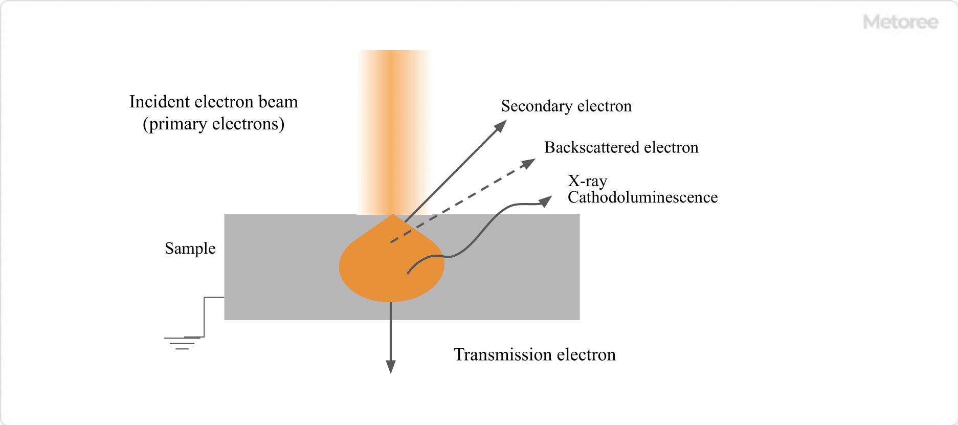
Figure 3. Example of electromagnetic waves emitted by electron beam irradiation
When a sample is irradiated with an accelerated electron beam, signals such as transmission electrons, X-rays, cathodoluminescence, and absorbed electrons as well as secondary electrons and backscattered electrons can be obtained. Analyzers may be attached to detect these signals.
Transmitted Electrons
If the thickness of the sample is thin enough or if the material is particulate, a portion of the irradiated electrons will be transmitted through the sample and can be detected as transmitted electrons. Generally, transmission electrons are measured by a transmission electron microscope or a scanning transmission electron microscope (STEM), which are independent measurement devices. Scanning transmission electron microscope (STEM) It is possible to observe internal structures that SEMs are not good at.
X-ray
When an atom is irradiated by an electron beam, X-rays are sometimes emitted in addition to electron beams. Since each atom has its own unique energy, it is possible to identify the type of atoms present on the sample surface by detecting the emitted X-rays.
There are two types of X-ray detectors: energy-dispersive X-ray detectors (EDS) and wavelength-dispersive X-ray detectors (WDS). Each has different characteristics and should be selected according to the purpose.
Cathodoluminescence
Cathodoluminescence is the light emitted when a sample is irradiated by an electron beam. By detecting this light, it is possible to measure the crystal properties of the sample, such as crystal defects, impurities, and carrier concentration.
Various other functions can be added by adding other options. Compared to the case where measurement is performed by an independent measurement device, the SEMs have the advantage that the measurement position can be selected while viewing the SEM’s image, allowing for more detailed measurement.