What Is Semiconductor Inspection Equipment?
 Semiconductor inspection equipment is equipment that inspects wafers and semiconductor chips for defects in the semiconductor manufacturing process.
The main semiconductor manufacturing processes include the photomask manufacturing process, which is equivalent to a printing plate, the wafer manufacturing process, which is the foundation of semiconductors, the front-end process of forming fine circuit structures on wafers using photomasks, and the back-end process of packaging individual semiconductor chips after circuit formation. If we look at the details, there are hundreds of processes.
In recent years, semiconductor microfabrication technology has reached the nanometer range (about 1/10,000th the thickness of a human hair), and at the same time, wafers have become larger in diameter, so that several thousand semiconductor chips containing billions of transistors can be produced from a single wafer.
Inspection equipment is extremely important in the semiconductor manufacturing process, which boasts such high productivity, leading to early rejection of defective products, cost reduction, and improvement of quality and reliability. The criteria for selecting semiconductor inspection equipment should take into consideration the diameter of the wafer, the process to be used, and the type of defects to be detected.
Uses of Semiconductor Inspection Equipment
Semiconductor inspection equipment is used in various phases of the semiconductor manufacturing process.
Defects to be detected using semiconductor inspection equipment include distortion, cracks, scratches, and foreign matter on photomasks and wafers, misalignment of circuit patterns formed in the front-end process, dimensional defects, packaging defects in the back-end process, and many other cases.
For this reason, it is necessary to select appropriate semiconductor inspection equipment and software for each process, and automation using AI, etc. is being promoted to speed up inspections and reduce manpower.
Principle of Semiconductor Inspection Equipment
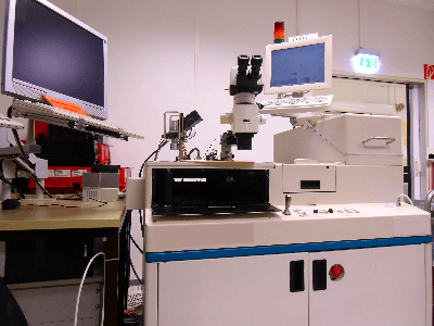
Semiconductor inspection equipment consists of measurement equipment, software to process the measured data, and facilities to perform the appropriate measurement.
High-resolution cameras, electron microscopes, and laser measuring instruments are used as measuring devices. Software for processing the measured data is developed with algorithms that are specific to the process to be inspected. Vibration suppression and lighting equipment are also necessary to ensure proper measurement. The image imaging, image processing, and defect classification technologies that are central to semiconductor inspection equipment are described below.
- Image Imaging Technology
Image imaging technology measures defects by irradiating a laser beam onto a wafer and then detects the scattered light. By illuminating minute irregularities, foreign matter and damage can be detected. - Image Processing Technology
Image processing technology is a technology that detects defects by comparing adjacent patterns, utilizing the fact that the patterns formed on all chips on the wafer are the same. It is capable of high-speed and wide-area processing. - Defect Classification Technology
Defect classification technology is a technology that, after detecting a defect, classifies the defect and extracts the cause. This technology is necessary to identify and address the causes of defects.
Types of Semiconductor Visual Inspection
1. Visual Inspection in Wafer Manufacturing Process and Front-End Process
Wafers are made from semiconductor raw materials such as silicon, which are formed as cylindrical monocrystalline materials called ingots, sliced to a thickness of about 1 mm, and polished on the surface, with a diameter of 12 inches (about 30 cm) these days.
Defects in wafers include not only attached foreign matter but also surface flaws, cracks, uneven processing, and crystal defects on the wafer itself, etc. Detecting these defects mainly by laser beam irradiation is the visual inspection in the wafer manufacturing process.
The front-end process proceeds in the wafer state, and there are two main types of defects that occur there, referred to as random and systematic. Random defects are mainly caused by the presence of foreign matter, but because they are random, their locations are unpredictable. Therefore, random defects on wafers are detected by image processing. Systematic defects, on the other hand, are defects caused by particles adhering to the photomask or exposure process conditions, such as on the photomask, and tend to occur at the same location on each semiconductor chip lined up on the wafer.
2. Visual Inspection in the Back-End Process
In the back-end process, wafers are cut into individual chips (dicing), placed in resin or ceramic packages, and sealed by connecting terminals on the chips to those on the package (wire bonding). The second stage of the process consists mainly of electrical inspections, but also includes visual inspections for wire bonding defects, part number printing defects, etc.
Other Information on Semiconductor Visual Inspection
1. Importance of a Semiconductor Visual Inspection
In general, visual inspections in the manufacturing process often aim to check for dirt, scratches, etc., and in some cases have nothing to do with product functionality or performance. However, dirt, scratches, etc. in semiconductor manufacturing are not merely apparent problems; in almost all cases, they are problems that affect functionality and performance.
Semiconductors are electronic devices, and like other electrical and electronic devices, electrical inspections are performed. However, it is extremely difficult to inspect all the billions of transistors and the wiring that connects them, and only visual inspections can confirm things like transistor gates and wiring detail.
2. Accuracy of a Semiconductor Visual Inspection
In semiconductor processes at the nanometer level, the thickness of a single wire and the spacing between adjacent wires are several nanometers.
If there are nano-order defects here, they can cause wiring shorts or wire breaks. Furthermore, even if the wiring width is 90% of the designed value due to a defect of 1/10th the size, the resistance and capacitance of the wiring will change. When an electric current flows through this wiring, a phenomenon called electromigration, in which metal atoms move due to the movement of electrons, occurs, rapidly thinning the wiring and causing disconnections to occur in a short period.
Thus, semiconductor manufacturing requires visual inspections with extremely fine precision, and as microfabrication technology continues to evolve, the required precision will continue to increase.