What Is a Prober?
 A prober is a device for fixing a probe (needle) at an arbitrary position, also called a probe station. It is a positioning device that connects the probe of the contact part of the measurement device to the correct position of the electrode of the semiconductor to measure electrical items on the semiconductor wafer in the front-end process, mainly in the semiconductor wafer manufacturing process and IC design and development.
Since the electrode area of a semiconductor is tiny, it is necessary to apply the probe of the contact part of the inspection device to the exact position. Very precise controllability is required for the prober in positioning.
In addition to semiconductor chips, this equipment is often used to evaluate the electrical characteristics of PCB substrates, various thin-film substrates, such as sensors and filters, and ceramic substrate packages, such as LTCC.
Uses of Probers
Probers are used when inspecting the electrical characteristics of semiconductors, thin-film substrates, and package substrates. When used for research and development purposes, the probers should have functions to eliminate noise and prevent signal leakage (crosstalk), be able to measure with high accuracy and be as versatile and flexible as possible in terms of measurement methods.
For mass production, the most important feature is the ability to perform fast processing accurately and in large quantities, so a wide variety of probers models should be selected to suit the application.
The probers must also be temperature tolerant to ensure correct operation at high and low temperatures during temperature characteristic evaluation. In addition, a prober that can handle high voltage and low impedance is required when used to measure semiconductors for power devices.
Principle of Probers
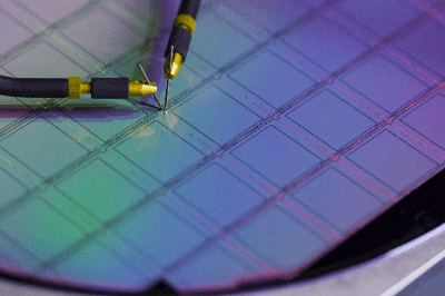
The most typical prober for silicon wafer applications is described below. The prober consists of a wafer chuck for fixing a silicon wafer, a stage for moving the wafer chuck in the XY direction, a contact plate to which multiple probes for inspection are attached and which moves in the Z direction concerning the stage, and a camera for positioning. The wafer is then moved in the XY direction to the stage.
In addition to these mechanisms, a transport system for moving silicon wafers is often included in probers products. The principle of operation is that when a silicon wafer is set, the silicon wafer is transported to the wafer check position and fixed.
The stage then positions the wafer in the XY direction, and with the position of the probe for measurement and the electrode of the semiconductor on the silicon wafer adjusted, the contact plate moves in the Z direction to contact the probe and the electrode. Through this process, the electrical characteristics of the semiconductor can be inspected by the inspection system.
Other Information About Probers
1. Miniaturization of Semiconductor Devices and Requirements for Probers
With the recent miniaturization of semiconductor devices, microcurrent measurement is an important indicator to evaluate the manufacturing quality of semiconductor devices. In the design and fabrication of semiconductor devices, changes in device materials, crystal growth parameters, or geometry can create unexpected current paths inside the device, which is commonly referred to as leakage current.
Increased leakage current can be caused by lattice defects, gate oxide structure, substrate selection, and other factors that can induce excessive power consumption and, in some cases, lower breakdown voltage. In recent years, the gate length of FETs and the emitter size of bipolar transistors in semiconductor devices have become very small, and while the voltage required to drive these devices is decreasing, leakage current is increasing.
Therefore, from the viewpoint of quality evaluation, highly accurate current measurements using probers are required. One measure to improve the accuracy is the development of cryogenic probes.
2. Positioning Accuracy of Probers and Positioners
The contact position accuracy of the probers directly affects the measurement accuracy. If various evaluations are performed without correct probing, it is difficult to know what is being evaluated.
For example, if you want to evaluate the characteristics of a semiconductor device, but the wafer is out of position and probed on an insulator, it is not difficult to imagine that the evaluation results will be far off from the expected results.
It is necessary to understand the accuracy required for the evaluation target and then focus on improving that accuracy. It is the component called a positioner (manipulator) that determines the positioning accuracy of the probers. Positioning accuracy varies depending on the correct selection of a positioner suited to the required specifications.
The specifications of a positioner are almost always determined by the following four factors: (1) travel distance, (2) travel resolution, (3) adjustment sensitivity, and (4) external dimensions. See below for the contents of each specification.
- Travel Amount
This is the amount of movement in the XYZ direction. Usually, it is described in the order of mm. - Travel Resolution
It is defined as the amount of movement per revolution. - Adjustment Sensitivity
Defined in terms of the minimum adjustable distance. In most cases, it is defined in μm. - External Dimensions
This is the size of the positioner, the will price increase in proportion to the size.
3. High-Frequency-Compatible Probers
Probers suitable for RF evaluation are required for the evaluation of semiconductor transistors for high-frequency (RF) and device modeling.
Generally, a GSG probe (a needle with a ground (GND) on both sides of the signal pad) with a dedicated calibration board is used, but depending on the frequency to be measured, care must be taken not only with the probe but also with the RF cable to the network analyzer or various measurement devices. This is because the flexure of the cable may affect the RF measurement results.
In the millimeter wave band, which has a higher frequency than a microwave, a dedicated VNA extender is used, but the configuration of the device should be discussed in detail with the dedicated manufacturer because the probers configuration itself has a very large impact on the measurement.