What Is a Field Effect Transistor (FET)?
Field effect transistors (FETs) are semiconductor devices in which the current flowing between source and drain is varied by applying a voltage to the gate electrode and controlling the flow of electrons or holes through the electric field of the channel.
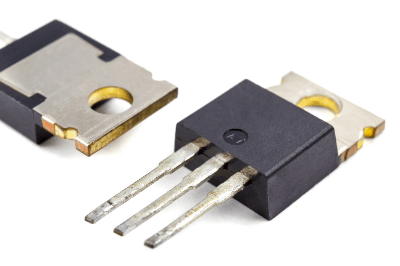
Field effect transistors (FET), like bipolar transistors, have three electrodes: the terminal corresponding to the base is the gate, the terminal corresponding to the collector is the drain, and the terminal corresponding to the emitter is the source, The terminal corresponding to the collector is the drain, and the terminal corresponding to the emitter is the source.
Uses of Field Effect Transistors (FETs)
Field effect transistors (FETs) are used in a wide variety of circuit fields. In digital circuits, FETs are used as elements in logic circuits. In analog circuits, they are often used in analog switches and electronic volume circuits, in addition to general amplifiers.
In particular, MOSFETs are suitable for integrated circuits because, in addition to their extremely low gate current, their structure is planar, and their manufacturing process is simpler and consumes less power than that of bipolar transistors. Large-scale digital integrated circuits, such as microcontrollers, are often composed of MOSFETs.
Field effect transistors (FETs) are also used as current switching elements in power electronics such as power supplies because of their low on-resistance and fast ON/OFF switching speed.
Principle of Field Effect Transistors (FETs)
The operating principles of JFETs and MOSFETs are different. In the following, the N-channel type is used as an example, but the P-channel type can be handled in the same way by reversing the polarity of the voltage applied to each electrode.
1. JFET
In the N-channel type, where the drain and source electrodes of the N-type semiconductor are connected to the gate electrode of the P-type semiconductor, applying a reverse voltage VGS (the gate electrode side is negative) to the PN junction between the gate and source electrodes causes a depletion layer to expand within the N-type region. Since there are no carriers in the depletion layer, the width of the current flow path (channel) in the N-type region narrows and the current ID flowing from drain to source decreases.
Based on this principle, ID can be controlled by changing the magnitude of VGS. Note that in this usage, the gate current hardly flows because of the inverse method voltage between the gate and the source. In other words, the input impedance is large.
2. MOSFET
MOS stands for metal-oxide-semiconductor. It has a three-layer structure consisting of a base semiconductor, an oxide layer as an insulating layer, and a metal electrode on top of the oxide layer. As mentioned in the previous section, there are two types of MOSFETs: enhanced type and depletion type.
In an N-channel enhancement type MOSFET with two N-type semiconductor regions in a P-type semiconductor, each of which is a drain and a source, no current flows because the drain and source are N-P-N before voltage is applied to the gate electrode. However, when a positive voltage is applied to the gate, negative charges collect under the gate through an insulating layer (oxide film) to form a thin layer of N-type semiconductor, and the drain-source interface becomes N-N-N, or continuous N-type semiconductor, allowing current flow.
The N-shaped semiconductor layer formed under the gate is called the “channel.” The thickness of the channel varies with the voltage VGS applied between the gate and the source, and the current ID flowing from the source to the drain varies with the thickness of the channel. In other words, ID can be controlled by the value of VGS. In addition, since the gate electrode is only in contact with the insulation layer, only a minute leakage current flows. This means that the input impedance is extremely large.
In the enhanced type, no current flows through the drain when VGS = 0 as described above, but in the depletion type, a thin channel is formed between the drain and source in advance to allow current to flow through the drain when VGS = 0. Therefore, Field Effect Transistors (FETs) are easy to use as amplification circuits because the drain current follows even when the signal level applied to the gate electrode is very small.
Types of Field Effect Transistors (FETs)
Field effect transistors (FETs) are classified according to their structure into junction field effect transistors (JFETs) and insulated gate field effect transistors (MOSFETs), which are indicated by different circuit symbols on the circuit diagram. There are also two types of MOSFETs: the P-channel type, in which two P-type semiconductor regions are embedded in an N-type semiconductor base, and the N-channel type, in which two N-type semiconductor regions are formed in a P-type semiconductor base, depending on the application.
Furthermore, MOSFETs can be classified into the enhancement type, in which no current flows between the source and drain unless a voltage is applied between the gate and source, and the depletion type, in which some current flows even when the gate and source are at the same potential.