What Is a Flip Chip Bonder?
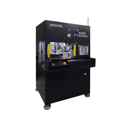
A flip chip bonder is a device used to mount various semiconductor devices on a substrate and is a new mounting technology that replaces conventional wire bonding. The term “flip chip bonder” is derived from the fact that semiconductor devices formed on a wafer are cut out (bare chip) and then flipped (flip) for bonding.
Almost all bare chip mounting has been replaced by flip chip bonding, which offers many advantages, and wire bonding continues to decline.
Uses of Flip Chip Bonders
Flip chip bonders are devices that bond and mount semiconductor devices onto substrates. While conventional wire bonding allows I/Os, the entry and exit points for signals, to be placed only on the periphery of the device, the flip chip method allows the entire underside of the device to be replaced with I/Os. This makes it possible to provide many I/Os, even with small appliances.
In addition, in the case of LEDs, where heat generation is a significant problem, the heat generated by the element can be dissipated directly to the substrate because it is mounted directly on the substrate without wires.
Principle of Flip Chip Bonders
Elements are cut from a wafer on which semiconductor elements are formed and then arranged on a flip chip bonder’s sorter (arranger), which inverts the elements. The inverted elements are then removed by a crimping device called a head and placed on the substrate with high precision by image processing.
In the ultrasonic method, which is currently widely used, ultrasonic waves are transmitted through the head to the protruding terminals called bumps on the backside (substrate side) of the element, which are instantaneously melted into the wiring pattern to achieve electrical continuity.
Sometimes, the space between the substrate and the device is filled with underfill resin. In such cases, the element and substrate are bonded using conductive adhesive instead of ultrasonic bonding.
Flip chip bonding and conventional wire bonding have the following advantages.
- High throughput because wires can be bonded in batches instead of connecting I/Os one at a time.
- High integration is possible because there is no chip-on-chip bonding, and no wire space is required around the chip’s perimeter.
- Suitable for high-speed signal processing due to low attenuation of high-frequency signals and signal loss caused by wires.