What Is a PIN Diode?
 A PIN Diode is a diode with a true I-type semiconductor of high electrical resistance between the P-type and N-type semiconductors and a wide depletion layer.
The wider depletion layer improves the response characteristics. The forward voltage is almost the same as that of a PN junction diode, and PIN Diodes are used as variable resistors, especially at high frequencies, because their resistance changes with the flowing current. They can also be used as capacitors when reverse voltage is applied.
Uses of PIN Diodes
PIN Diodes have low capacitance between terminals, low series resistance, and high frequency characteristics. Therefore, they are used for switching high-frequency signals such as those used in cellular phones, since they do not easily affect high-frequency communication lines. It is also used in band switching, AGC circuits, and receiving attenuators as a variable resistor because of its ability to change resistance in response to current. It also acts as a capacitor when a reverse voltage is applied.
Principle of PIN Diode
1. When a Forward Voltage Is Applied to a Pin Diode
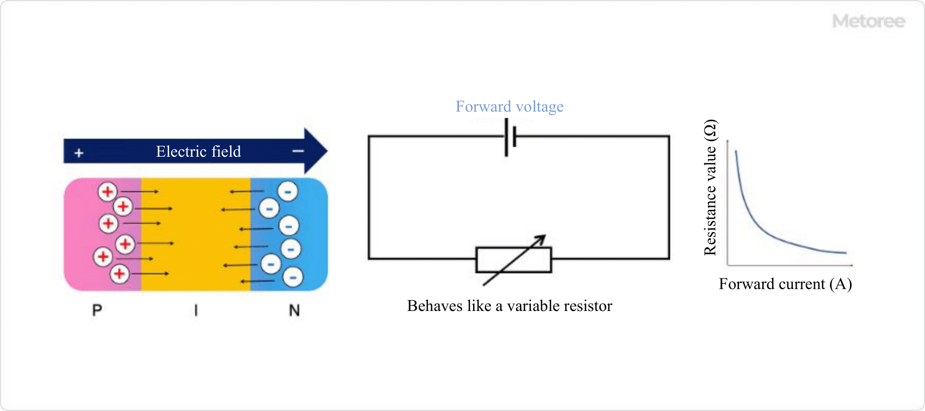
Figure 1. Forward voltage applied to the PIN diode
When a forward voltage is applied to a PIN Diode, holes from the P-type semiconductor and electrons from the N-type semiconductor move into the I-type semiconductor, where they meet and recombine. The holes and electrons from the P-type and N-type semiconductors meet in the I-type semiconductor, resulting in a change in resistance. In other words, the resistance changes in response to voltage, making it possible to use the device as a variable resistance by controlling the voltage.
In addition, by changing the thickness and area of the depletion layer of the I-type semiconductor, the capacitance between terminals can be varied and the resistance characteristics can be selected Compared to PN-type semiconductors that do not have an I-type semiconductor, PIN Diodes have improved performance because they are more effective in accumulating carriers such as holes and electrons.
2. When a Reverse Voltage Is Applied to a Pin Diode
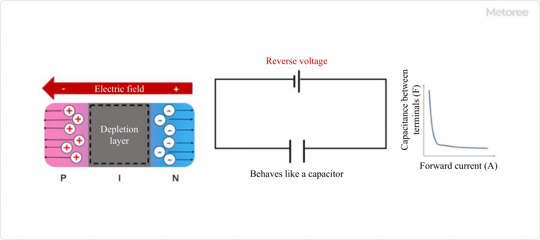
Figure 2. Reverse voltage applied to PIN diode
On the other hand, when a reverse voltage is applied, holes and electrons gather on the P-type and N-type surfaces respectively, and the I-type semiconductor becomes a dielectric and acts as a capacitor.
Other Information on PIN Diodes
1. Conductivity Modulation of Pin Diode
Conductivity modulation refers to the change in resistance due to the flow of carriers into the high-resistance layer when biased.
The I layer, sandwiched between the P and N layers, consists of elements with tetravalent valence, such as silicon (Si) and germanium (Ge). These are called true semiconductors because they are pure semiconductors containing no other elements. They are insulating layers in which electrons cannot move because they are bound by stable covalent bonds with eight electrons.
However, when forward biased in a PIN Diode, holes flow from the P layer and electrons flow from the N layer, and the I layer becomes highly doped. As a result, conductivity modulation occurs and the I layer, which had high resistance, becomes low on-resistance as current flows in the forward direction.
2. Switches with PIN Diodes
PIN Diodes are also used in high-frequency switches. While mechanical switches are also available in the low-frequency range, coaxial relays and semiconductor switches are used in the high-frequency range. In recent years, they are also used as millimeter-wave band MMIC switches due to the spread of LAN communication systems and in-vehicle radar systems.
The principle of PIN Diode switch circuits is that high-frequency signals are output during forward bias and no high-frequency signals are output during reverse bias. Both reflective and absorptive types exist in the product lineup. Reflective switches transmit high-frequency power during reverse bias and reflect it during forward bias. Absorptive switches have a low voltage standing wave ratio (VSWR) and low signal loss in both ON and OFF modes.
3. Advantages and Disadvantages of PIN Diode Switches
In general, PIN Diode switches are superior in terms of switching speed and small size, but they have the disadvantage of high power consumption.
The reason for the large power consumption is the need to apply a high bias to minimize insertion loss. To compensate for this disadvantage, an optical switch called MEMS (Micro Electro Mechanical System) has been developed for the millimeter wave band and is gaining market share in today’s market.