What Is a Photoetching Process?
A photoetching process is a processing technology that combines the principle of photography (photoengraving technology) and etching technology to remove unnecessary parts.
It can form complex and fine patterns on materials, such as substrates.
Uses for a Photoetching Process
The photoetching process has the following applications:
1. Electronic Board Fabrication
It is used to produce printed circuit boards that are built into most electronic devices. Printed circuit boards consist of copper foil attached to a base made of ceramics or resin. Unnecessary portions of the copper foil are removed by photoetching to produce electronic circuits.
Other uses include the production of flexible circuit boards (FPCs) and rigid circuit boards used in electrical products and cell phones. Components are used in circuit boards for touch sensors, temperature sensors, antennas, heaters, and camera sensors.
2. Fabrication of Electronic Circuits
It is used for fine patterning of semiconductors and liquid crystal displays.
3. Manufacture of Precision Parts
Used as a metal mask (stencil) to print solder paste on printed circuit boards in the surface mounting process where many electronic components are mounted.
Principle of Photoetching Processes
The photoetching process generally involves the following steps:
1. Mask Production
Draw mask patterns on glass and other materials.
2. Resist Coating on Substrate
A resist (photosensitive film) is applied to the substrate to be etched. Resist must be coated in a dark room, as it is altered by light.
3. Exposure and Development
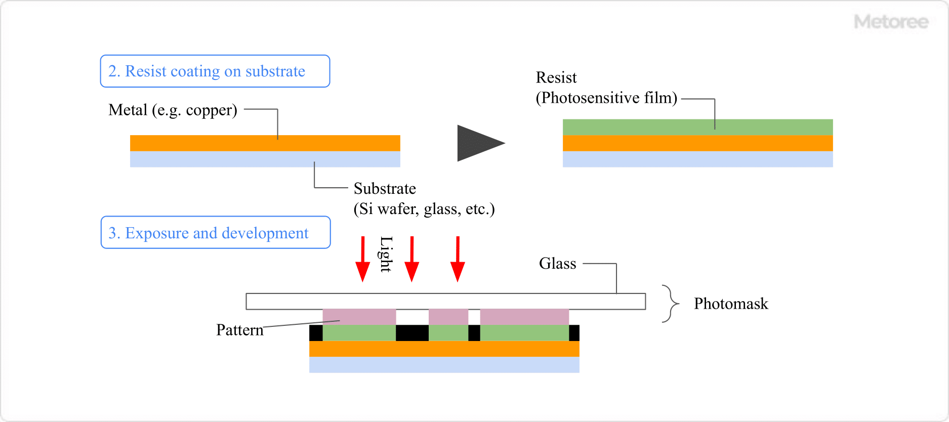
Figure 1. Resist coating on substrate and exposure/developing
Expose with the mask created in step 1 placed on the resist coat. The area not covered by the mask is transformed and can be removed by the developer (only in the case of positive type. In the case of negative type, the unexposed areas will be removed by the developer).
4. Etching
The metal in the area where the resist was removed in step 3 is removed with an etchant. Etching on silicon substrates, for example, uses highly corrosive hydrofluoric acid as the etchant, so care must be taken when handling it.
5. Resist Removal and Cleaning
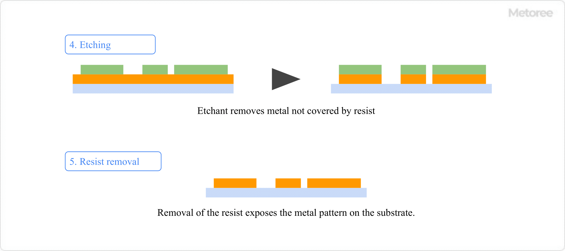
Figure 2. Etching and resist removal
The resist is removed and cleaned to complete the process.
Types of Photoetching Process
1. Metal Etching
After removing dirt from the material to be processed (stainless steel, copper, nickel, etc.), photoresist is applied to the reverse side of the material. After masking with a photomask, the photoresist is exposed to UV light to sensitize the photoresist.
Next, the photoresist is removed from the areas that were not illuminated by the photomask using specified chemicals. Finally, a metal-dissolving chemical (etchant) is used to dissolve the unmasked areas to obtain the pattern as designed.
2. Precision Hybrid Etching
This is a processing technique that combines etching and electroforming (a technique to create a model opposite to the master product). This processing technology makes it possible to manufacture precision products.
3. Etching of Special Materials
This method is used to etch very hard metals such as molybdenum and titanium.
4. 3D Etching
This is a method of etching three-dimensional or curved surfaces. Etching is performed on the inside of cylindrical products and on the outside of bar-shaped products.
5. Thin Film Etching
This is a method for etching thin metal films (ITO, Al, Cu, Ni, Cr, etc.) formed by vapor deposition or sputtering using a chemical process to form patterns with high processing accuracy.
Other Information on Photoetching Process
Photomask Fabrication Method
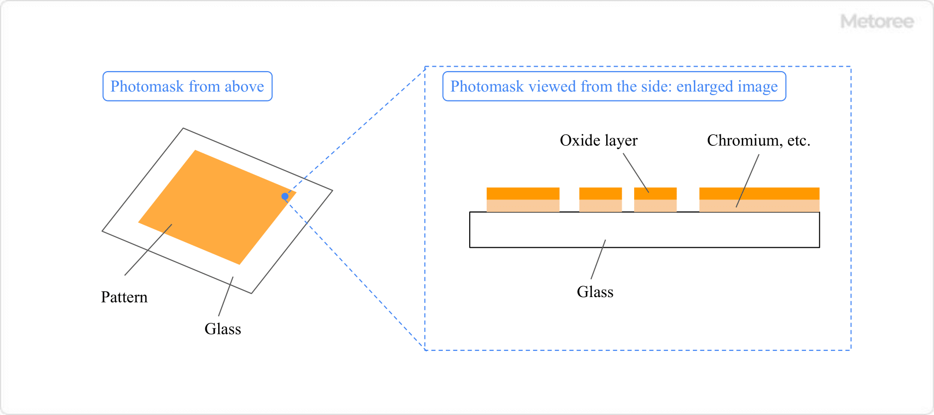
Figure 3. Photomask Structure
The photomask fabrication process is similar to that of photoetching. First, a pattern is drawn by CAD or other means. Next, a substrate with some kind of light-shielding film on a glass substrate is prepared.
There are three types of light shielding films: chrome mask, glass mask, and film mask, in order of processing accuracy. These substrates are called photomask blanks.
Next, resist is applied to the photomask blanks, and an electron beam or other means is used to draw the original mask that will become the basis of the product. Thereafter, in a process similar to photoetching, the light-shielding film is removed by a developer solution, and finally the resist is removed and washed.