What Is Plasma CVD System?
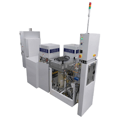
Plasma CVD equipment is a type of equipment that performs a type of chemical vapor deposition method.
Plasma CVD stands for plasma-enhanced chemical vapor deposition. The raw material gas is turned into a low-temperature plasma state (glow discharge ionized into cations and electrons) to generate active ions and radicals that cause chemical reactions on the substrate to deposit and form a thin film.
Uses of Plasma CVD Systems
Plasma CVD technology is used for reinforcing films for cutting tools (titanium nitride, carbon nitride, DLC (diamond-like carbon)), semiconductor insulating and protective films, wiring and electrode materials (silicon nitride, silicon oxide, copper, aluminum, tungsten, polycrystalline silicon, compound semiconductors, etc.). These materials are used as insulators, protective films, wiring and electrode materials (silicon nitride, copper, aluminum, tungsten, polycrystalline silicon, compound semiconductors, etc.). Its use in high-performance power devices to control and supply energy, which is key to economic and industrial development, is also expanding rapidly.
The supply gas for plasma CVD systems is usually a carrier gas such as hydrogen, nitrogen, argon, or ammonia mixed with a raw material gas such as SiH4 (silane) or WF6 (tungsten hexafluoride).
1. Oxides
Silicon dioxide (SiO2) is an oxide of silicon. It has excellent electrical insulation and thermal stability and is used in semiconductor device interlayer insulating films.
As semiconductors become thinner, they are more prone to leakage currents, where current leaks out from unplanned locations; the presence of SiO2 helps prevent leakage currents.
2. Nitride
Silicon nitride (Si3N4) is a nitride of silicon. It has excellent strength and thermal conductivity and is used as a substrate material for power devices that generate a lot of heat.
Nitrogen and ammonia are used together with SiH4 to form nitrides, so they also play the role in raw material gases. Semiconductors in general perform functions related to arithmetic and memory, such as memory. Power devices, on the other hand, are for things like diodes.
3. Carbide
Silicon carbide (SiC) is a carbide of silicon, a member of the compound semiconductor family along with GaN (gallium nitride, or GaN), AlGaN, etc. Like Si3N4, it is used in power devices in place of Si IGBTs because of its superior strength and thermal conductivity.
Compared to silicon compounds, power loss is lower, leading to smaller devices.
4. Metals and Metal Compounds
The gate of a transistor is formed from a gate oxide film (formed by thermal oxidation) and a gate electrode (mostly polycrystalline silicon). Tungsten plugs used for the gate electrode and source-drain contacts are formed by plasma CVD. (See Figure 3)
Principle of a Plasma CVD System
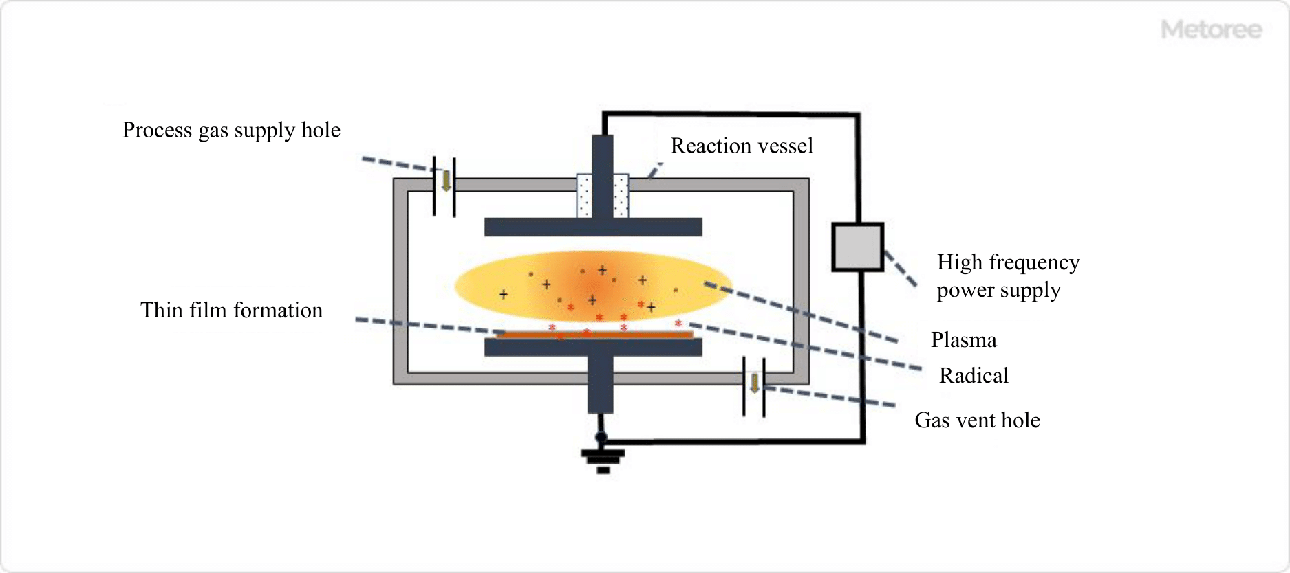
Figure 1. Basic configuration of a plasma CVD system
The raw material gas is selected from a pressure reduction range of 10-4 to 100 Pa, depending on the desired conditions. The power supply frequency most commonly used for plasma excitation is 13.56 MHz (RF: Radio Frequency), and the discharge type is a capacitively coupled type using parallel plate electrodes.
One of the parallel plates may be used as a shower head to supply process gas, or a heater may be inserted in one of the plates to control the temperature. There are many controllable parameters, such as power supply frequency, electrode structure other than the parallel plate type, raw gas composition, discharge volume, and temperature. Therefore, it is possible to deposit various types of thin films with various functionalities, ranging from inorganic to organic materials.
Other Information on Plasma CVD Systems
1. Semiconductor Device Structure and Manufacturing Process
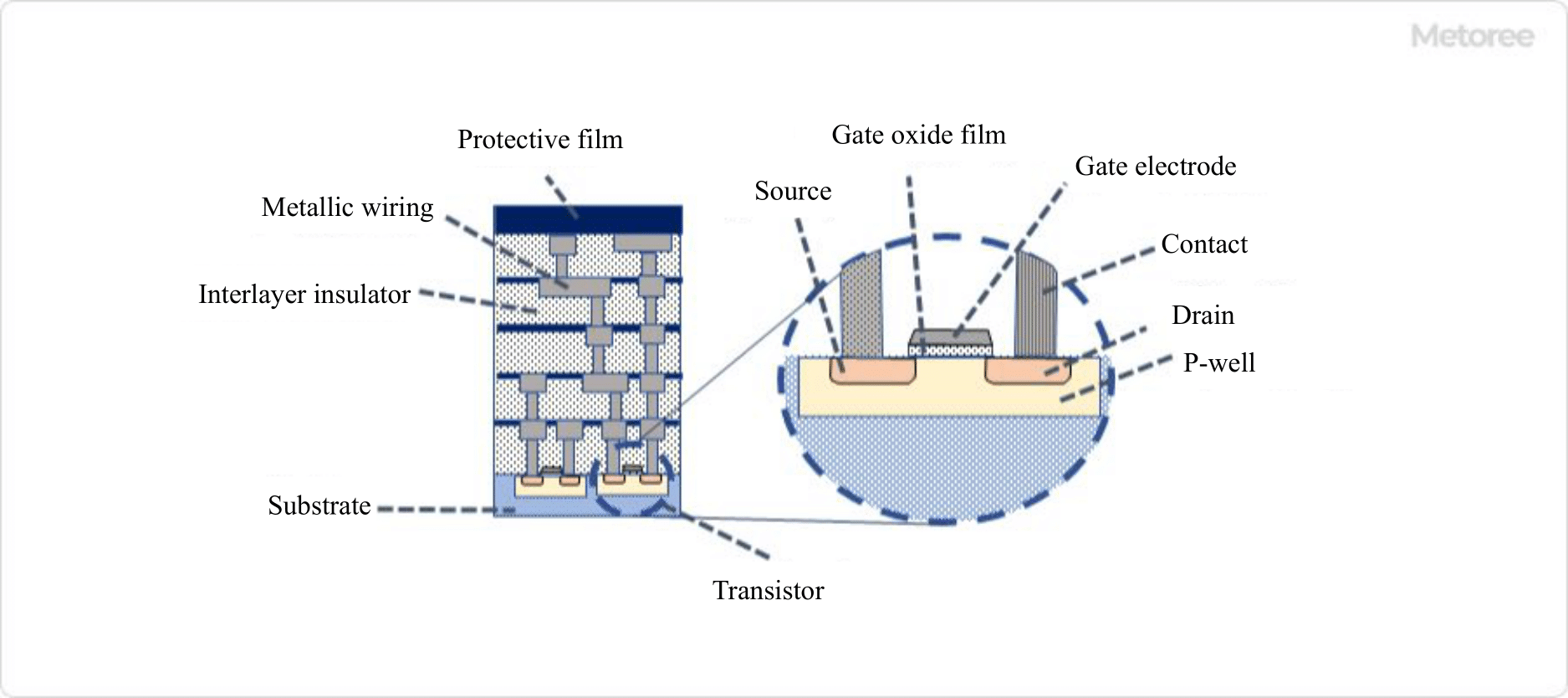
Figure 2. Basic structure of semiconductor devices (memory)
Plasma CDV systems are widely used in the manufacture of semiconductor devices. For example, in the case of memory devices, complex multilayer wiring is formed on top of the MOSFET (metal oxide semiconductor field-effect transistor) formed on the substrate (wafer). layers are formed on top of the MOSFET (metal oxide semiconductor field-effect transistor) formed on the substrate (wafer) and separated by an interlayer insulating film.
Plasma CVD systems are mainly used to form MOSFET gate electrodes, wiring layers, and interlayer insulators, which require fine patterning after deposition. Basically, printing technology is used for patterning, and the following steps are repeated.
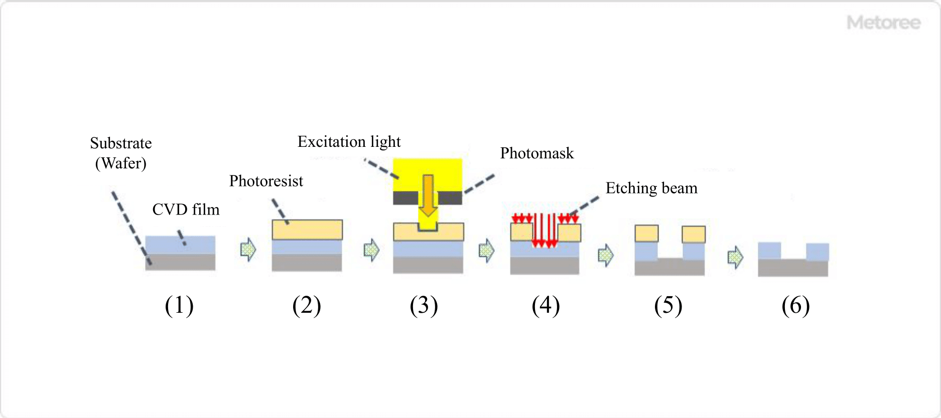
Figure 3. Basic deposition process for semiconductor devices
- On top of the base pattern, a new pattern material (polycrystalline silicon, Al, C, W, SiO2, Si3N4, etc.) is uniformly deposited by CVD.
- A photoresist film (positive or negative) is formed on top of the first film.Positive films are less soluble in solvents due to excitation light, while negative films are more soluble.
- The resist is dissolved, forming a pattern of the remaining resist on top of the deposited film.
- Etching (stripping process) is applied from the top of the pattern to remove the film.
- Remove the resist.
- A pattern is formed on the film.
By repeating the above process, semiconductor devices can be formed.
2. Thermal CVD and Optical CVD
Depending on the energy given, it can be classified into plasma CVD, thermal CVD, and optical CVD.
- Thermal CVD
This is a method of film deposition in which the components are thermally decomposed and chemically reacted by treating the feed gas at high temperatures. (This method cannot be used for substrates that are sensitive to heat, such as plastics. - Optical CVD
Methods that use laser light or ultraviolet light energy to activate family decomposition and chemical reactions.