カテゴリー
category_kr

필름 커패시터

필름 커패시터란?

필름 커패시터는 플라스틱 필름을 유도체로 사용하는 커패시터를 말합니다. 그 기술적 뿌리는 19세기 후반에 발명된 종이 커패시터로 거슬러 올라갑니다. 종이 커패시터는 알루미늄 호일에 기름이나 파라핀 종이를 끼워 롤 형태로 감아 넣습니다.

종이에 직접 금속을 증착하여 감은 타입을 MP(메탈라이즈드 페이퍼) 커패시터라고 한다. 필름 커패시터는 이러한 기술을 바탕으로 1930년대에 개발되었습니다.

필름 커패시터는 내부 전극의 구조에 따라 호일 전극형과 증착 전극형(금속화 필름형)으로 나뉘며, 구조의 차이에 따라 권취형과 적층형, 유도형과 무유도형으로 나뉩니다.

필름 커패시터의 사용 용도

필름 커패시터는 민생용품부터 산업기기까지 다양한 제품에 사용됩니다. 민생용품의 예로는 냉장고 등 가전제품과 내비게이션, 카 오디오, ETC 등 차량 내 탑재 전자기기 등이 있습니다. 산업기기의 예로는 파워 일렉트로닉스 기기 등에 사용됩니다.

필름 커패시터는 절연 저항이 강하고 안전성이 높다는 특징이 있습니다. 또한, 무극성 및 고주파 특성이 우수하고, 온도 특성도 우수합니다. 또한, 정전 용량을 고정밀도로 대응할 수 있고 수명이 깁니다.

그러나 필름 커패시터는 적층 세라믹 칩 커패시터에 비해 크기가 커집니다. 따라서 세라믹 커패시터로 커버할 수 없는 전압 및 용량 영역이나 고성능, 고정밀 위기에 사용되는 경향이 있습니다.

필름 커패시터의 원리

커패시터는 원래 전기를 저장하거나 방출하는 전자 부품입니다. 마주보는 전도체 사이에 전압을 가하면 그 사이에 끼어있는 절연체 또는 공간에 정전기 유도 작용이 일어납니다. 정전기 유도 작용에 의해 절연체에 유전체 분극이 발생해 충전됩니다.

그 유도체에 필름을 사용한 것이 필름 커패시터입니다. 필름 커패시터는 내부 전극의 구성과 구조의 차이에 따라 몇 가지로 나뉩니다.

1. 호일 전극형 필름 커패시터

내부 전극이 되는 금속박에 플라스틱 필름을 겹겹이 감은 권취형 필름 커패시터입니다. 금속박의 재질은 알루미늄, 주석, 구리 등을 사용합니다.

호일 전극형 필름 커패시터는 유도형과 무유도형이 있습니다. 유도형의 경우 내부 전극에 리드선을 부착하여 권취하는 반면, 무유도형은 단면에 리드선 또는 단자 전극을 부착합니다. 무유도형은 유도형에 비해 인덕턴스 성분을 작게 할 수 있어 고주파 특성이 우수합니다.

2. 증착 전극형 필름 커패시터

플라스틱 필름에 금속을 증착하여 내부 전극을 만드는 타입의 필름 커패시터입니다. 금속 재료로는 알루미늄이나 아연을 사용합니다. 증착막은 매우 얇기 때문에 호일 전극형 필름 커패시터보다 소형화가 가능합니다.

필름 커패시터의 기타 정보

1. 필름 커패시터의 극성

필름 커패시터에는 극성이 없습니다. 즉, 필름 커패시터는 무극성 커패시터입니다. 고정 커패시터는 무극성 커패시터와 극성 커패시터 두 종류가 있습니다.

  • 무극성 커패시터
    단자에 양극과 음극의 구분이 없는 커패시터가 무극성 커패시터입니다. 어느 쪽 단자가 양수이든 상관없습니다. 단자에 가해지는 전압의 극성이 조절되지 않습니다. 무극성 커패시터라면 교류 회로에서도 직접 사용할 수 있습니다.

    필름 커패시터는 무극성 커패시터의 주류 중 하나입니다. 무극성 커패시터에는 세라믹 커패시터, 종이 커패시터, 운모 커패시터, 공기 커패시터 등이 있습니다.

  • 극성 커패시터
    두 단자 중 어느 쪽이 양극이 될지 정해져 있는 커패시터가 유극성 커패시터입니다. 단자의 극성을 잘못 사용하면 커패시터가 파손될 수 있습니다.

2. 필름 커패시터와 오디오

오디오 기기는 소리를 원하는 대로 만들기 위해 직접 제작하거나 커스터마이징을 할 수 있습니다. 음질을 좌우하는 요소는 여러 가지가 있지만, 사용 부품도 음질을 좌우합니다. 커패시터는 그 부품 중 하나입니다.

오디오 앰프에 사용되는 커패시터에 요구되는 특성은 다음과 같습니다.

  • 고주파 특성이 좋을 것
  • 고조파 왜곡이 적을 것
  • 소위 말하는 울림이 적을 것

필름 커패시터는 전해 커패시터에 비해 위의 특성에 대해 우수합니다. 음질에 있어서도 전해 커패시터에 비해 필름 커패시터가 음의 투명도나 해상력이 우수합니다.

カテゴリー
category_usa

Screening Test

What Is a Screening Test?

A screening test refers to the preliminary sorting of products or chemicals to prioritize samples for detailed testing. These tests serve various purposes, including assessing disease risk, pharmaceutical development, substance toxicity, and identifying defective semiconductor products.

Uses of Screening Test

Screening tests have broad applications in semiconductor development, pharmaceuticals, toxicity assessments, and more.

1. Exclusion of Initial Defects in Semiconductors

Precision electronic components like semiconductors undergo extensive screening tests, including visual, electrical, and environmental stress screenings. Products that pass these tests are shipped as finished goods.

2. Initial Development of Pharmaceuticals

In pharmaceutical development, screening tests help select potential pharmaceutical compounds from a large pool of candidates. These tests evaluate compounds’ effects on receptors, enzymes, ion channels, and proteins to identify effective pharmaceuticals.

3. Risk Assessment of Chemical Substances

Screening tests under chemical regulations assess the risks posed by chemical substances, focusing on environmental pollution, toxicity to humans, animals, and plants, residue absence, and explosion or ignition risks. Substances that cannot be confirmed as safe may be designated as priority assessment chemicals.

4. Initial Assessment of Allergy Labeling

Screening tests are crucial for food allergy labeling, ensuring the safety of allergy patients. Two different screening tests verify the validity of food allergy labeling on processed food products.

5. Parts for Satellites, Rockets, Among Others

Components used in aerospace applications, such as satellites and rockets, undergo rigorous reliability tests and screening to prevent failures. Screening test methods are established to ensure their reliability.

Principle of Screening Test

The term “screening” implies sorting. Screening tests involve the selection or testing process through medical or chemical experiments. Some tests can be burdensome and costly. In such cases, screening tests are conducted on the entire population to identify potential risks. There are three main types of screening tests: visual screening, electrical screening, and environmental stress screening. The choice of method depends on the target and environmental factors.

Characteristics of Screening Tests

Screening tests aim to identify potential risks using relatively simple methods while minimizing financial and physical burdens. However, false positives may occur, leading to further detailed testing to confirm or rule out issues.

カテゴリー
category_kr

SiC MOSFET

SiC MOSFET이란?

SiC MOSFET은 기존의 Si 기판이 아닌 화합물 반도체인 SiC(실리콘 카바이드) 기판을 사용한 MOSFET을 말합니다.

전계효과 트랜지스터의 일종인 MOSFET의 반도체 기판 재료로 사용되며, MOSFET은 온/오프 스위칭, 증폭기 등의 용도로 사용됩니다. 재료로 사용하는 반도체 기판에 화합물 반도체인 SiC를 사용함으로써 기존 Si MOSFET에 비해 전압을 인가한 상태에서의 저항값을 낮출 수 있습니다.

그 결과, 턴오프 시 스위칭 손실과 전력 동작 시 전력 손실을 작게 억제할 수 있습니다. 반도체 칩의 성능 향상과 트랜지스터 동작 시 필요한 냉각 용량을 줄일 수 있기 때문에 제품 자체의 소형화로 이어질 수 있습니다.

SiC MOSFET의 사용 용도

SiC MOSFET은 파워일렉트로닉스 분야의 전자기기 등 릴레이, 스위칭 전원, 이미지 센서 등 많은 반도체 제품에 사용되며, SiC MOSFET을 채용하면 스위칭 오프 시 손실 감소로 인해 고속 스위칭이 가능하여 통신기기에 사용되는 경우가 많다. 통신기기에도 사용되는 경우가 많습니다.

SiC MOSFET을 선정할 때는 제품 애플리케이션의 동작 상태, 즉 절대 최대 정격 및 전기적 특성, 패키지 사용 및 크기 등을 고려해야 합니다.

SiC MOSFET의 원리

SiC MOSFET은 동일한 내압을 유지하면서 낮은 ON 저항과 턴오프 시 저손실 동작이 가능한 MOSFET 구조를 구현할 수 있습니다. 이는 Si 기판에 비해 약 3배의 밴드갭 에너지와 약 10배의 파괴전계 강도의 물성치를 갖는 SiC 기판을 재료로 사용한 트랜지스터이기 때문에 활성층의 층 두께를 얇게 만들 수 있기 때문입니다.

SiC MOSFET은 p형 반도체와 n형 반도체가 적층된 구조를 가지고 있습니다. 보통 p형 반도체 위에 n형 반도체를 적층하고, n형 반도체에는 드레인과 소스 전극, n형 반도체 사이에는 산화절연층과 게이트 전극이 부착되어 있습니다. 또한, 본체의 실리콘 웨이퍼에는 화합물 반도체인 SiC(실리콘 카바이드)가 에피 기판으로 사용됩니다.

MOSFET은 게이트에 양의 전압을 인가하면 소스와 드레인 사이에 전류가 흐른다. 이때 실리콘 웨이퍼에 SiC를 사용하는 SiC MOSFET은 Si만 사용하는 MOSFET에 비해 소스와 드레인 사이의 전압과 전류를 크게 해도 동작할 수 있습니다. 반도체의 불순물 농도를 높일 수 있기 때문에 손실 감소 및 소형화가 가능합니다.

SiC MOSFET의 기타 정보

1. SiC MOSFET과 IGBT와의 구분

IGBT는 일반 Si MOSFET이 대응하기 어려운 고전력 영역의 사용 용도에 사용되는 트랜지스터이지만, 최근 이 영역에 SiC MOSFET 디바이스가 사용되고 있습니다. 그 이유는 SiC의 밴드갭 에너지가 커서 IGBT에 비해 고온 동작이 가능하기 때문입니다. 또한, IGBT의 경우 후단 바이폴라 트랜지스터의 스위칭 손실이 크다는 문제를 해결할 수 있는 것도 이유 중 하나입니다.

이전에는 SiC 에피 기판이 소구경이어서 양산성과 비용 측면에서 어려움이 있었다. 하지만 최근에는 8인치 대응이 가능해져 양산성과 가격도 개선되고 있는 상황입니다.

10kW 이상의 비교적 큰 전력을 다루는 애플리케이션, 예를 들어 전기차(EV) 용도, 발전 시스템 용도, 주택용 전력 용도 등에 적극적으로 활용되고 있습니다.

2. SiC 디바이스와 GaN 디바이스의 차이점

SiC와 함께 주목받고 있는 와이드 밴드갭 반도체로 GaN(질화갈륨)이 있는데, GaN은 SiC에 비해 밴드갭 에너지가 더 크고, 절연파괴 강도도 큰 소자로 연구기관을 중심으로 활발한 연구가 진행되고 있습니다.

GaN은 일반적으로 Si 기판 위에 GaN의 활성층을 형성하는 구조이기 때문에 SiC MOSFET과 같은 고출력 응용 분야에는 대응하기 어렵습니다. 시장에서는 1KW급 전력을 다루는 애플리케이션에서 비교적 많은 연구가 이루어지고 있습니다. 예를 들어, 5G 기지국용 고출력 증폭기 용도나 PC 및 USB를 통한 배터리 충전 용도로 많이 사용되고 있습니다.

GaN 디바이스도 SiC MOSFET과 마찬가지로 고온 동작이 가능하고, 냉각 장치나 과도한 배열 구조가 필요 없어 소형 PC 전원 어댑터로 최근 널리 보급되고 있습니다.

カテゴリー
category_kr

클럭 버퍼

클럭 버퍼란?

클럭 버퍼는 어떤 인쇄 회로 기판의 시스템 내에서 클럭이 여러 논리 회로에 도달하기까지의 지연 차이를 최대한 줄여 타이밍을 맞추는(동기화) 데 사용되는 IC입니다.

여러 개의 논리 회로를 동작시키는 경우, 회로 간 동기화가 필요합니다. 이때 시스템 전체를 제어하는 신호가 필요한데, 이를 위해 사용되는 일정한 주파수의 주기적인 신호가 바로 클럭입니다 (음악의 메트로놈과 같은 역할을 합니다).

클럭에 연동하여 동작하는 회로군을 동기화 회로라고 합니다. 클럭은 시스템 내에서 분기되어 수많은 논리 회로로 전파된다. 그러나 이 클럭이 동기화되지 않으면 논리 회로의 오작동으로 인해 시스템 전체가 원하는 동작을 하지 못하게 될 수 있기 때문에 클럭 버퍼가 필요합니다.

클럭 버퍼의 사용 용도

클럭 버퍼는 컴퓨터, 통신 시스템, 산업용 기기 등 다양한 분야에서 사용됩니다.

구체적인 사용 용도는 다음과 같습니다.

  • 디지털 논리 회로 (CPU, FPGA 등)
  • 데이터 컨버터 (아날로그 ⇔ 디지털 변환)
  • 고속 인터페이스 (USB, Serial-ATA, PCI-Express 등)
  • 무선 시스템의 주파수 변환

일례로 컴퓨터 동작의 핵심인 CPU(Central Processing Unit)를 예로 들면, 클럭 신호에 의해 각 회로(제어장치, 연산장치, 레지스터, 저장장치와의 인터페이스, 입출력 장치와의 인터페이스)를 동기화하여 동작을 제어하고 있습니다.

또한, 어느 용도든 여러 회로 간의 정보 및 데이터 교환을 보다 정확하게 동기화하는 것이 안정된 동작을 위해 필수적입니다.

클럭 버퍼의 원리

클럭 버퍼는 회로 방식에 따라 ‘Non-PLL Buffer’와 ‘PLL Buffer’로 분류됩니다.

내부적으로 PLL(phase-locked loop: 위상동기 루프)을 사용하느냐의 여부가 큰 차이점이며, PLL은 입력되는 주기적인 신호에 피드백 제어를 가하여 다른 발진기로부터 위상이 동기화된 신호를 출력하는 회로를 말합니다. 다음과 같습니다.

  • Non-PLL Buffer
    PLL을 거치지 않고 입력 신호를 분배하기 때문에 지터 열화(주기적인 흔들림)가 적습니다.
  • PLL Buffer
    입력 신호와 출력 신호 사이의 지연이 매우 작습니다.

클럭 버퍼는 클럭 신호를 여러 개 출력할 수 있으므로, 클럭 신호원과 클럭 버퍼를 각각 1개씩만 준비하면 같은 주파수의 클럭으로 동작하는 여러 회로군에서 사용할 수 있는 클럭을 생성할 수 있습니다.

따라서 부품 비용의 절감과 프린트 기판의 레이아웃을 용이하게 할 수 있다는 장점이 있습니다. 그 외에도 일부 제품에서는 레벨 변환이 가능하고, 설정이 용이하다는 특징도 있습니다.

클럭 버퍼를 선택하는 방법

입력 신호의 요구 사양, 출력 클럭의 주파수, 신호 수, 전압, 지터, 스큐, 입출력 간 지연, 클럭 버퍼의 전원 전압, 패키지 외형 치수, 핀 수, 소비전력, 비용 등을 디바이스의 데이터시트에서 확인한 후, 설계하는 시스템에 가장 적합한 디바이스를 선정합니다.

시스템 내 각 회로군에 분배되는 클럭이 100% 동일한 타이밍에 스위칭되는 것이 이상적이지만, 현실적으로 실현 가능한 경우는 거의 없습니다. 하지만 회로의 오동작을 방지하기 위해 우수한 특성을 가진 디바이스를 선정하는 것이 중요합니다.

클럭 버퍼에 대한 추가 정보

클럭 버퍼의 사용법과 역할

시스템 내에서 안정적으로 사용할 수 있는 클럭을 생성하기 위해서는 클럭 신호원과 이를 보완하고 여러 회로군에 적절히 분배할 수 있는 클럭 제품이 필요합니다.

1. 클록 신호원

클록 신호원으로는 공진기나 발진기가 사용됩니다. 공진기란 고유 주파수를 가진 진자를 말합니다.

단독으로 동작하지 않으며, 세라믹, 수정, SAW의 범주로 나뉩니다. 발진기는 진자를 진동시키기 시작해 진동을 지속시키는 회로(발진회로)와 공진기를 패키지로 만든 제품을 말합니다. 수정, SAW, 실리콘, MEMS 발진기 등이 있습니다.

2. 클럭 제품

클럭 신호원을 보완하는 클럭 제품 중 하나가 클럭 버퍼입니다. 발진기의 출력 신호를 클럭 버퍼에 입력합니다. 그 입력 신호와 동일한 주파수의 클럭 신호를 여러 개 출력하는 것이 클럭 버퍼의 역할입니다. 
오실레이터를 보완하는 클럭 제품에는 이외에도 클럭 제너레이터(다중 주파수 생성 가능), 지터 클리너(지터 성능 개선), RF 신시사이저(고주파수 출력) 등이 있으며, 설계자는 사양과 비용 등 시스템에 요구되는 요구사항에 따라 선택해야 합니다.

カテゴリー
category_kr

스프링 핀 커넥터

스프링 핀 커넥터란?

스프링 핀 커넥터는 서로 다른 부품 간에 전기를 흐르게 하는 접점으로 사용되는 전기 커넥터 부품 중 하나입니다.

기본적으로 핀, 튜브, 스프링으로 구성되어 있습니다. 핀과 연결된 튜브 안에 스프링이 들어 있어 진동에 강하고, 흔들림이 있어도 접촉 장애가 잘 발생하지 않는 것이 특징입니다.

미세 피치 커넥터, 저저항 모듈형 커넥터, 하우징이 있는 제품 등 종류가 다양합니다. 극수, 접점 수, 접점 높이 등도 다양하고 내구성도 좋으며, 원터치로 탈부착이 가능한 제품도 많습니다.

스프링 핀 커넥터의 사용 용도

스프링 핀 커넥터는 모바일 기기나 운송기기에 활용되고 있습니다. 스프링 핀 커넥터는 스프링에 의해 진동을 받아도 접촉이 잘 유지되기 때문에 진동을 받는 제품에는 필수적입니다.

우리 일상에서 무선 이어폰의 충전 박스, 2in1 태블릿 PC의 태블릿 단말기와 키보드 연결, 스마트워치 충전, 전기자동차 충전 커넥터 등에 사용됩니다. 스프링 핀 커넥터는 기기의 소형화에도 기여합니다.

예를 들어, 기판과 기판 또는 기판과 배터리를 연결하는 용도로도 적합합니다. 그 외에도 크래들, 내부 안테나 연결도 그 중 하나다. 표면 실장형, 스루홀형, 솔더컵형이 있으며, 납땜으로 기판과 연결합니다.

스프링 핀 커넥터의 원리

스프링 핀 커넥터는 스프링의 힘으로 전기 접점 간의 접촉을 유지합니다. 기본적으로 3개의 부품으로 구성되며, 본체인 중공형 배럴, 배럴 내부에 수납되는 코일형 스프링, 스프링에 의해 상대 부품에 눌려지는 플런저의 3개 부품으로 구성됩니다.

스프링과 플런저 사이에 볼, 쉘, 인슐레이터라는 부품을 넣은 4부 구조의 타입도 있습니다. 스프링 핀 커넥터의 구조는 포고 핀 구조라고도 합니다.

스프링으로 반발하는 구조가 포고스틱이라는 손잡이와 계단을 달고 스프링의 힘으로 점프하는 막대 모양의 놀이기구를 닮았다고 해서 붙여진 이름입니다. 플런저, 배럴은 황동이 많이 사용되며, 스프링에는 SUS나 피아노선이 많이 사용됩니다. 또한 접촉면의 표면 처리는 금도금이 주류를 이룹니다.

스프링 핀 커넥터의 기타 정보

1. 스프링 핀 커넥터의 결합 방향

스프링 핀 커넥터를 이용한 부품의 결합은 수직 방향으로 결합하는 것이 바람직합니다. 수직방향이 아닌 수평방향으로 부품끼리 슬라이딩하도록 연결하면, 플런저는 스프링을 누르는 방향과 90° 어긋난 방향으로 배럴에 대해 쓰러지려는 힘이 작용합니다.

만약 스프링이 아래로 내려가지 않으면 배럴의 가장자리가 손상될 수 있습니다. 그러나 수평 방향의 결합을 고려한 조치를 취하면 수평 방향의 결합도 가능합니다.

그러나 일반적으로 견딜 수 있는 결합 횟수가 줄어들고 슬라이드에 의한 도금의 마모도 커지므로 슬라이드 거리를 최대한 짧게 하거나 도금 두께를 두껍게 하는 등의 대책이 필요합니다.

2. 스프링 핀 커넥터의 사양

스프링 핀 커넥터에는 용도에 따라 특수 기능을 향상시킨 사양이 있습니다. 대표적인 3가지 사양을 소개합니다.

방수 대응
제품이 물에 젖을 가능성이 있는 경우에는 방수 사양의 스프링 핀 커넥터가 선택된다. 방수를 위해 포팅, O-링, 고무 시트 등의 방수 부품이 사용됩니다.

고속 전송 지원
전자기기에서는 정보 전달이 이루어지며, 기기의 성능 향상을 위해 데이터의 고속 전송이 필수적입니다. 스프링 핀 커넥터를 사용하여 대량의 데이터를 고속으로 전송하는 경우, 커넥터 전자기장 해석을 통해 핀 배열 등의 사양을 설계합니다.

고전류 대응
스프링 핀 커넥터 중에는 고전류 연결에 사용되는 것도 있습니다. 소형 스프링 핀 커넥터에서도 대량의 전류가 흐를 수 있도록 접촉 면적을 확보하고 발열을 억제하기 위해 볼, 절연체 등의 부품이 내장되어 있습니다.

カテゴリー
category_kr

GaN 전력소자

GaN 전력소자란?

GaN 전력소자는 질화갈륨 결정 위에 형성된 차세대 반도체 전력소자로, 기존 실리콘 위에 형성된 전력소자보다 더 큰 전력을 더 적은 손실로 처리할 수 있어 최근 주목받고 있습니다.

기존 실리콘 위에 반도체 공정으로 만든 전력 소자보다 더 큰 전력을 더 적은 손실로 처리할 수 있어 최근 주목받고 있으며, GaN 전력소자는 그 구조상 실리콘계 전력 소자에 비해 신뢰성과 안전성이 실용화되기까지 많은 어려움이 있었습니다. 하지만 최근 화합물 반도체 관련 기술 혁신으로 이러한 문제가 해결되고 있습니다.

GaN 파워 디바이스의 고효율화를 통해 배열기구의 단순화 등도 가능해 제품의 대폭적인 소형화 및 저소비전력화에 기여할 수 있습니다.

GaN 파워 디바이스의 사용 용도

GaN 파워 디바이스는 스마트폰이나 PC의 급속 충전을 가능하게 하는 충전기나 휴대폰 기지국용 앰프에 널리 사용되고 있습니다. 실리콘계 파워 디바이스보다 더 큰 전력을 처리할 수 있기 때문에 이를 대체하는 용도로 PC 충전기나 기지국용 증폭기 등에 사용되는 경우가 많습니다.

또한, 태양광 발전 시스템 등의 파워 컨디셔너에서는 매우 높은 변환 효율이 요구되기 때문에 고효율의 GaN 파워 디바이스가 채용되기 시작했습니다. 또한, 고속 스위칭 동작이 가능하기 때문에 전원 안정성이 요구되는 서버 기기 등의 스위칭 전원으로도 사용되고 있습니다.

GaN 파워 디바이스의 원리

GaN 파워 소자의 원리는 밴드갭이라는 반도체 물성치가 Si에 비해 GaN은 약 3배 이상 높은 전계를 견디는 소자이기 때문에 소자의 단위 면적당 동작 가능한 전력(전력) 밀도를 매우 크게 확보할 수 있다는 점에 있습니다.

일반적으로 GaN 파워 소자는 HEMT 구조라고 불리는 고전자 이동도 트랜지스터 회로로 구성됩니다. 이 HEMT 구조는 항상 전류가 흐르는 노마리 ON 상태이며, 게이트에 음전압을 가하면 OFF가 됩니다. 따라서 어떤 결함으로 게이트 전극에 음전압을 인가할 수 없게 되면 OFF가 되지 않아 매우 불안정한 상태가 됩니다.

GaN 파워 디바이스는 이러한 신뢰성 문제가 있어, 안정적인 노멀리 OFF를 실현하는 것이 사용성 측면에서 과제였습니다. 그래서 게이트 전극에 노멀리 OFF가 가능한 Si-MOSFET을 내장하여 노멀리 OFF를 실현하고 있습니다.

또 다른 과제로는 전류 붕괴라는 물리 현상을 들 수 있습니다. GaN 파워 디바이스는 Si나 SiC 웨이퍼 위에 GaN 필름을 형성시켜야 하는데, 결정 박막 성막 기술의 혁신으로 현재는 고품질 성막이 가능해졌습니다. 가능하게 되었습니다.

GaN 전력 소자의 기타 정보

1. GaN과 SiC의 차이점

GaN과 SiC는 밴드갭이 커서 절연 파괴 강도가 커서 소자 내압을 높이기 쉽습니다. 따라서 고전류, 고전압 애플리케이션에 적합합니다. 특히 SiC는 디바이스의 내전압 측면에서 EV 자동차, 발전 시스템 등 모터 구동 용도 등 고전류용 애플리케이션에 많이 사용되며, 향후 IGBT를 대체할 수 있는 디바이스로서 큰 기대를 받고 있습니다.

한편, GaN 파워 디바이스는 SiC만큼의 내압은 확보하기 어렵지만, 특히 고주파 특성을 나타내는 Cut off 주파수(fT)가 높고, 전자의 이동도가 커서 빠른 스위칭 속도와 고주파 동작이 요구되는 애플리케이션에 널리 사용되고 있습니다.

즉, GaN과 SiC의 구분은 고속 스위칭 충전이나 고주파수 용도의 5G 기지국용은 GaN 소자를, 고내압, 고전류 용도는 SiC 소자를 사용하는 것으로 구분할 수 있습니다.

2. GaN을 이용한 전력 반도체 트렌드

GaN 전력 반도체는 크게 두 가지로 나뉘는데, 현재 비교적 높은 650V 이상의 전기차 온보드 충전용과 하이브리드 전기차의 48V에서 12V로의 DC-DC 컨버터에서 전압 변환을 위한 애플리케이션이 그것입니다. 두 가지 모두 GaN 전력 반도체로서 SiC 디바이스와 함께 향후 WBG(Wide Band Gap) 디바이스 시장을 주도할 것으로 예상됩니다.

이러한 신규 애플리케이션 용도를 위한 실용화 과제는 신뢰성, 제조 수율, 비용이지만, 전 세계 반도체 관련 기업들의 노력으로 실용화 가능성은 크게 진전되고 있습니다.

3. GaN 소자의 응용 분야

GaN 디바이스의 또 다른 응용 분야로는 광원용 응용을 들 수 있는데, GaN은 화합물 반도체 중에서도 직접 전이형 반도체이기 때문에 발광 효율이 높은 LED 광원이나 레이저 다이오드용 재료로서 큰 기대를 받고 있습니다.

전자 소자로도 고출력이며, 밀리미터파 및 Sub-THz용 고주파수용 증폭 트랜지스터로 응용이 기대됩니다.

カテゴリー
category_usa

AMS Test

What Is an AMS Test?

AMS test, also known as the Ames test, is an examination that assesses whether a chemical substance can induce mutations in genes (mutagenicity) using bacteria.

Uses of AMS Test

The Ames test (mutagenicity test) is conducted to detect the mutagenic properties of chemical substances. It is commonly employed in safety evaluations during the development of new pharmaceuticals and pesticides, assessing their safety. Additionally, when there is a concern that a chemical substance may cause health hazards in the environment, the Ames test is used for its evaluation.

Due to regulations such as the Industrial Safety and Health Act, Pharmaceutical Affairs Law, and the Pesticide Control Law, the implementation of genotoxicity tests, including the AMS test, is mandatory for assessing the safety of chemical substances that may pose harmful effects to human health or the environment.

Principle of AMS Test

1. Principle

The principle of the AMS test involves using bacteria that have been genetically modified to be incapable of synthesizing amino acids, thus making them dependent on externally supplied histidine. Chemical substances are added to the medium in which the bacteria reproduce, and a genetic mutation test is performed to detect bacteria that have undergone spontaneous mutations. Chemical substances with higher mutagenicity are known to induce more mutations.
As many carcinogens are mutagenic, the strength of their mutagenic effects can be used to assess their carcinogenic potential. The size and formation of bacterial colonies are examined to determine the mutagenic properties of the sample.

2. Test Method

Specifically, strains of Salmonella typhimurium with a histidine requirement are used. These strains are mutants that cannot grow unless histidine, an essential amino acid, is provided in the environment. The histidine-requiring strains are cultured in a medium containing the chemical substance.
If the chemical substance is mutagenic, mutations occur during bacterial division, allowing the bacteria to produce histidine on their own. As a result, the bacteria proliferate and form colonies, and by measuring the number of colonies, the mutagenic nature of the substance can be determined.

3. Association with Carcinogenicity

While the AMS test examines the mutagenic properties of chemical substances, it does not determine whether they cause cancer. However, as a significant portion of known carcinogens are mutagenic, the results of the AMS test may be used to assess potential carcinogenicity. Nevertheless, determining carcinogenicity solely based on the AMS test results is not feasible, and a comprehensive judgment is required by combining results from other types of tests.

Types of AMS Test

There are two types of AMS tests: direct test and indirect test.

In a direct test, chemical substances directly affect bacteria. In contrast, an indirect test evaluates chemical substances after passing through metabolic organs like the liver, where they produce metabolites indicating mutagenicity. To enhance metabolic activation, a reagent called “S9 mix,” obtained by treating rat liver, is added to the medium containing bacteria and the chemical substance.

Other Information on AMS Test

Testing Regulations

In Japan, domestic guidelines (Pharmaceutical Affairs Law, Pesticide Control Law, Industrial Safety and Health Act, etc.) stipulate the implementation of preliminary and main tests. On the other hand, OECD chemical guidelines, used in Europe and elsewhere, require the repetition of the main test under identical conditions as part of the reproducibility confirmation. Combining the preliminary test and main test results involves conducting the test three times.

The cost of testing chemical substances for carcinogenicity through animal experiments is substantial. The AMS test is rapid, relatively low-cost, and offers the advantage of accurately evaluating the mutagenicity of chemical substances. However, as the test uses bacteria, it cannot assess the complex reactions or side effects present in living organisms, compared to animal experiments.
カテゴリー
category_usa

Aging Test

What Is an Aging Test?

Aging Test

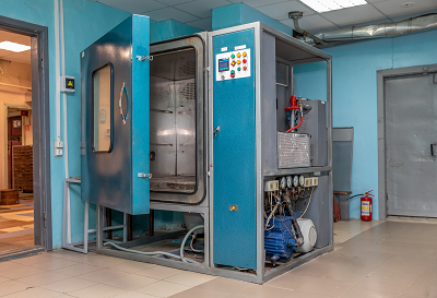
An aging test refers to an examination where products undergo intentional degradation through continuous operation under harsh conditions. These conditions include exposure to high temperatures, low temperatures, high humidity, and heavy loads over an extended period. The primary purpose of this test is to assess the durability and lifespan of the product.

Typically, aging tests are an integral part of pre-shipment testing and validation during new product development. They play a crucial role in quality assurance.

The aging test process involves subjecting products to conditions that accelerate wear and tear, allowing for the early detection of potential failures. Simulating extreme conditions helps manufacturers evaluate how well their products can withstand real-world usage over an extended period.

This type of testing has gained significance, particularly with the trend toward product miniaturization. Understanding how increased heat generation affects the lifespan of smaller devices is essential for producing reliable and durable products.

As a result, the demand for aging tests has been steadily increasing as manufacturers strive to ensure the longevity and quality of their products.

カテゴリー
category_usa

EMC Test

What Is an EMC Test?

EMC Test

EMC test, or electromagnetic compatibility (EMC) test is an examination conducted to verify the performance of EMC.

EMC test consists of two components: the EMI (Electromagnetic Interference) test and the EMS (Electromagnetic Susceptibility) test. EMI test measures the electromagnetic waves emitted by electronic devices and similar equipment to the external environment. This test ensures that the levels of electromagnetic waves radiated into space from electronic devices comply with specified standards.

Specifically, the test measures electromagnetic waves emitted to the external environment through radiation or conduction from electromagnetic waves or power and communication harnesses. On the other hand, the EMS test evaluates the resistance of electronic devices to external electromagnetic waves.

In the EMS test, external noise such as static electricity and radiated electromagnetic fields is applied to electronic devices. The test verifies whether electronic devices operate normally even when subjected to noise within the specified standards.

Uses of EMC Test

EMC test is conducted to meet the standards set by EMC regulations and specific EMC standards for various countries and regions. During the pre-sale product development stage, the purpose is to perform EMC tests as defined by the standards and confirm compliance.

Once the standards are met, electronic devices can be sold in the market.

Principle of EMC Test

EMC test adheres to international standards established by the IEC (International Electrotechnical Commission) and its committee, CISPR (International Special Committee on Radio Interference). While IEC primarily focuses on EMS test standards, CISPR concentrates on EMI test standards.

EMC regulations in various countries and regions are based on IEC and CISPR standards. The United States and Europe have stringent regulations on EMC through legal measures. In Japan, there are no specific regulations regarding EMC, and industry organizations like VCCI have adopted voluntary regulatory measures.

Types of EMC Test

1. Radiated Emission Test

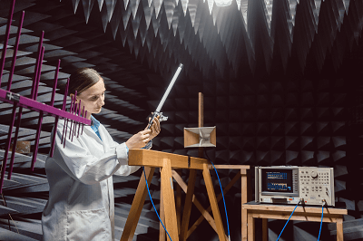
Quantifies electromagnetic waves radiated from electronic devices using an antenna and verifies if the measured values are within predetermined standards. The test is conducted in a radio wave darkroom or open site, measuring frequencies above 30MHz.

2. Conducted Emission Test

Quantifies electromagnetic waves conducted and radiated from the power or communication lines of electronic devices using a spectrum analyzer. The test is conducted in a radio wave darkroom or shield room, measuring frequencies from 9kHz to below 30MHz.

3. Electrostatic Discharge Immunity Test

The test checks if electronic devices operate normally when subjected to static electricity. The test is conducted by applying static electricity from an electrostatic discharge gun to electronic devices.

There are direct discharge tests where static electricity is applied directly to electronic devices and indirect discharge tests where static electricity is applied from conductive objects near electronic devices.

4. Radiated Electromagnetic Field Immunity Test

This test verifies if electronic devices operate normally when exposed to high-frequency electromagnetic waves. The test is conducted in a radio wave darkroom or open site, using a test antenna to apply frequencies above 80MHz to electronic devices.

5. Electrical Fast Transient/Burst Immunity Test

This test checks if electronic devices operate normally when transient abnormal voltages occur during the interruption of coils or inductors. The noise is applied to the power or communication lines of electronic devices.

For the power line, noise is applied to the electronic device’s inlet. For the communication line, the electronic device’s communication harness is clamped using a coupling device, and noise is applied to the communication line.

6. Surge Immunity Test

This test checks if electronic devices operate normally when transient abnormal voltages occur during lightning strikes or ON/OFF switching of switches. The noise has a longer cycle than transient bursts. A dedicated test apparatus is used to apply noise to the power or communication lines of electronic devices.

カテゴリー
category_usa

Ferric Chloride Etching

What Is Ferric Chloride Etching?

Ferric Chloride Etching

Ferric chloride etching is a method of wet etching, a process used to shape the surface of materials such as metals, glass, and ceramics. This technique involves removing material through erosion by solutions, differing from dry etching, which uses gases and beams.

Ferric chloride (FeCl3) solution is used in this wet etching method, being suitable for almost all metals except a few, like titanium.

Uses of Ferric Chloride Etching

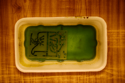
Ferric chloride etching is widely used in metal processing for its precision compared to traditional machining methods. It’s particularly prevalent in the electronics industry for creating detailed wiring patterns on printed circuit boards (PCBs) and manufacturing IC lead frames. This technique is also used in the fine processing of metals and ceramics in various manufacturing industries and art for copper plate etching in printmaking.

Principle of Ferric Chloride Etching

The process begins by applying a resist to parts of the metal surface that should remain unetched. On PCBs, this is typically done using metal resists like solder or tin, or organic resists such as ink or film.

When the material is immersed in ferric chloride solution, an oxidation-reduction reaction occurs, where copper transforms into cuprous chloride (CuCl), and ferric chloride reduces to ferrous chloride (FeCl2). This reaction involves electron exchange between copper atoms and ferric ions, resulting in the removal of copper from the surface.

After etching, the resist is stripped using acidic solutions for metal resists or alkaline solutions for organic resists. Finally, the substrate is cleaned to remove any remaining chemicals or resist residues.