What Is a Silicon Wafer?
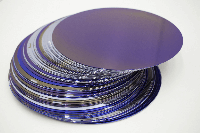
Silicon wafer is a material for semiconductor products. Silicon means silicon and a wafer is a thinly sliced cylinder. Therefore, a silicon wafer is a thinly sliced silicon single crystal.
Silicon is a typical material for electronic devices. Electronic devices support our lives. As the demand for electronic devices increases, the need for silicon wafers will also increase.
Uses of Silicon Wafers
Though we may not be aware of the uses of silicon wafers in our daily lives, they are in all electronic devices. Silicon wafers are used as substrates for semiconductor products. Typical examples of the use of semiconductor products are listed below.
- Office automation equipment such as smartphones and personal computers
- Control units of mobile equipment such as automobiles and aircraft
- AI and robot internals
- Solar batteries
Principle of Silicon Wafers
Silicon wafers are fabricated from the element silicon. Silicon is the second most abundant element on the earth’s surface after oxygen. It is a common element found in soil and rocks, but using quartz, the material for silicon wafers is refined.
A cylindrical silicon rod called a silicon ingot is used to make silicon wafers. Silicon wafers are produced by slicing silicon ingots into thin slices.
Silicon ingots are made from high-purity silicon crystals using two major methods: the CZ method (Czochralski method) and the FZ method (Floating Zone method).
- The CZ Method
In the CZ method, raw silicon materials are melted in a high-temperature furnace at temperatures exceeding 1,000℃. A silicon ingot is completed when a seed silicon rod is inserted into the furnace and levitated while rotating at high speed.
- The FZ Method
The FZ method uses polycrystalline silicon material in rod form. The raw material is attached to the seed monocrystalline silicon material, and the boundary surface is inductively heated. The polycrystalline silicon material becomes monocrystalline, and a silicon ingot is completed.
Other Information on Silicon Wafers
- Silicon Wafer Manufacturing Process
Silicon wafers are manufactured using silicon ingots produced by the above two methods. The manufacturing process is as follows:
- Cutting of Ingots
- Ingots are cut using diamond blades to produce wafers of the desired thickness.
- Polishing of Wafers
- To maintain the quality of the circuit pattern, the surface of the wafer is polished to a mirror-like finish. Thus, it is free of particulates and other impurities.
One of the reasons for the significant development of large-scale integrated circuits using silicon semiconductors is the establishment of a technology that enables the mass production of high-purity, defect-free silicon single-crystals at a relatively low cost. The manufactured silicon is of ultra-high purity of 99.999999999% or higher and is called “eleven-nine” because there are eleven nines in a row.
Silicon ingot fabrication technology also continues to improve. Ingots have so far grown in diameter from 20 mm to 200 mm.
- Silicon Wafer Market Share
The global electronics market is expanding yearly, and the semiconductor industry is becoming increasingly essential to support this growth. The market for silicon wafers was $11.9 billion in 2018.
Silicon Wafer Share by Consumption Region
The market shares by consumption region are South Korea (35%), North America (29%), Taiwan (16%), China (10%), and Japan (7%), with higher shares in North America, South Korea, and Taiwan, where semiconductor manufacturers are based.
Silicon Wafer Sales Share by Vendor Nationality
The share by vendor nationality is Japan (55%), Taiwan (20%), Germany (14%), and South Korea (10%), with Japanese companies holding a high share.
2020 “Survey on Industrial Infrastructure of Electronic Equipment Manufacturing” from Ministry of Economy, Trade and Industry data.