カテゴリー
category_usa

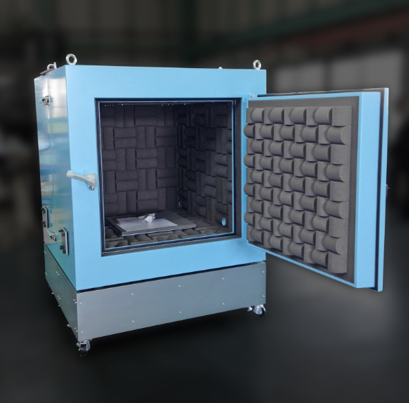
Acoustic Anechoic Box

What Is an Acoustic Anechoic Box?

An anechoic box has two properties: sound insulation and sound absorption.
It blocks sound waves coming from outside the box, while it does not reverberate sound inside the box. It is used to measure sound waves generated by compact driving components such as motors and fans, and electrical equipment using a sound level meter or analyzer.

How to use an Acoustic Anechoic box

The acoustic anechoic box is used in combination with a sound level meter and analyzer. A microphone cable is connected to a measuring instrument installed outside the box and a microphone is set inside the box via a cable port in the anechoic box. The generated sound of a DUT (device under test) is measured by operating the measuring instrument outside the box.

Difference between an Acoustic Anechoic chamber and an Acoustic Anechoic box

Unlike an anechoic chamber, there are no requirements by ISO standards on its design and measurement, but it is used for the purpose of a simplified measurement. However, correlative and comparative measurements are feasible by making corrections based on the master data acquired in an anechoic chamber.

Technical specifications required to an Acoustic Anechoic box

The background noise inside an anechoic box should be a very quiet environment. It may be preferable for the background noise to be at least 10 dB lower than the measurement sound of DUT. In other words, when the measurement sound is 30 dB, the environment inside the anechoic box should be quieter than 20 dB. Therefore, the anechoic box is required to have high sound insulation value.

Measuring instruments used in the Acoustic Anechoic box
and reliable measuring instrument manufacturers

The measuring equipment used in combination with the anechoic box should be selected according to the sound generated by DUT, and relatively high-performance microphone and analyzer are required as well.
Reliable measuring instrument manufacturers: Hottinger Brüel & Kjær, GRAS, Siemens, Onosokki, Rion…etc.

カテゴリー
category_usa

Programmable-Gain Amplifier

What Is a Programmable-Gain Amplifier?

A programmable-gain amplifier is an amplifier that allows the user to change the magnitude of gain by programming.

It is an amplifier that uses operational amplifiers and generally has a non-inverting configuration. Because the gain can be adjusted through programming, programmable-gain amplifiers leave room for change in the signal chain, where analog signals are converted to digital signals.

This leads to the development of flexible products since it is possible to respond flexibly to customer or user wishes, such as increasing the signal reception strength, by changing the gain later.

Uses of Programmable-Gain Amplifiers

Programmable-gain amplifiers are mainly used for signal amplification in devices that receive signals or noise, such as communication equipment, detectors, and analyzers. Examples include base stations and receivers for cellular phones, ultrasonic radar, wireless communications, and voice analysis. Other applications include motor control.

When selecting specifications for programmable-gain amplifiers, the range and type of programmable gain, impedance magnitude, and gain accuracy should be considered.

Principle of Programmable-Gain Amplifiers

Programmable-gain amplifiers use a ladder configuration of resistors in the negative feedback circuit section of operational amplifiers and switch these resistor values via switch operation by controlling the register values of digital circuits. This enables gain switching and amplifier operation with a wide dynamic range.

In addition to the resistance value of the negative feedback circuit section, another technique is to change the internal voltage applied to the op amp by programming, which allows the amplification factor of the op amp itself to be varied to change the magnitude of gain. Programmable-gain amplifiers for equipment used in medical devices and scientific experiments require amplifiers with a large dynamic range, low noise, and excellent temperature stability.

For this reason, some products incorporate resistors or capacitors in the programmable-gain amplifiers to form a low-pass filter and eliminate high-frequency noise. Also available are products that connect multiple operational amplifiers with a circuit that has a programmable switch, etc., so that the operational amplifiers can be operated by the program as needed, enabling efficient and large amplification.

Other Information on Programmable-Gain Amplifiers

1. Programmable-Gain Amplifiers Used in Sensor Applications

In the design of a system using sensors, the output range of various types of sensors is designed to match the input range of the A-D converter in the subsequent stage, but the input-output range in the system does not always match. In such cases, programmable-gain amplifiers should be used between the sensor and the A-D converters to cover the sensor’s very low output range at very low levels and match the input range of the A-D converters.

In the case of sensor applications, noise levels must naturally be taken into account due to their application role. Instrumentation amplifiers are also often used, but programmable-gain amplifiers can be thought of as instrumentation amplifiers with an additional variable gain function in the second stage.

2. Difference Between Programmable-Gain Amplifiers (PGA) And Variable-Gain Amplifiers (VGA)

Both are the same in the sense that they are amplifiers whose gain can be changed and adjusted. Programmable-gain amplifiers (PGAs) are used for gain adjustment of discrete (precise) values because they are digitally controlled and bit-switched (4x, 8x, 16x, etc.) rather than continuously adjusted in an analog fashion.

Note that there is only as much adjustment resolution in the gain setting as the number of bits in the adjustment register. A variable gain amplifier (VGA), on the other hand, is an analog, continuous gain control with a relatively fast response and is suitable for applications that require AGC (automatic gain control) operation.

カテゴリー
category_usa

Semiconductor Lithography Equipment

What Is Semiconductor Lithography Equipment?

Semiconductor Lithography Equipment is used to depict circuit patterns on silicon wafers in the semiconductor manufacturing process. A powerful ultraviolet light is transmitted through a photomask, which serves as a prototype for the circuit pattern, and the circuit pattern is transferred onto a silicon wafer coated with photoresist. In recent years, some equipment uses a laser with a wavelength of 13 nm, called EUV, to miniaturize fine circuit patterns. Since extremely high precision is required for positioning, etc., the equipment is expensive.

Applications of Semiconductor Lithography Equipment

Semiconductor Lithography Equipment is used in the exposure process of manufacturing integrated circuits (ICs), which include semiconductor devices such as MOS (metal oxide semiconductor)-FETs (field effect transistors).

In the IC manufacturing process, photolithography and etching cycles are repeated sequentially on a silicon wafer to stack and process layers (layers) of silicon oxides and metals in a predetermined pattern, which are processed to have the characteristics required for semiconductor devices. In the case of n-type MOS (NMOS), for example, an n-type (n+ type) MOS is formed by forming a silicon oxide film in the gate region on a p-type silicon substrate and a gate metal on top of it, and ion implanting high concentration impurities in the drain and source regions. Each of the photolithography and etching steps in this series of processes is configured as shown in the figure (film deposition process S1~resist stripping process S6).

Of these, the exposure process (S3) is the process performed using Semiconductor Lithography Equipment. Different wavelengths of exposure equipment are used depending on the dimensions of the circuit pattern and the accuracy of the Semiconductor Lithography Equipment.

Principle of Semiconductor Lithography Equipment

Semiconductor Lithography Equipment consists of a light source, condenser lens, photomask, projection lens, and stage. Ultraviolet light generated from the light source is adjusted by the condenser lens so that they face the same direction. The ultraviolet light then passes through a photomask, which serves as a prototype for one layer of the circuit pattern, and the light is reduced by the projection lens to transfer the circuit pattern (one layer of the circuit pattern) of the semiconductor device onto the silicon wafer. In an exposure system such as a stepper, once the transcription is completed, the silicon wafer is moved by the stage and the same circuit pattern is transferred to another position on the silicon wafer. By replacing the photomask, another layer of the circuit pattern of the semiconductor device can be transferred.

KrF excimer lasers with a wavelength of 248 nm, ArF excimer lasers with a wavelength of 193 nm, and EUV light sources with a wavelength of 13 nm are used as light sources.

The design rule (minimum processing dimension) for the latest semiconductor manufacturing process has been miniaturized to 3 to 5 nm, so high precision on the nanometer scale is required for all condenser lenses, photomasks, projection lenses, and stages. Also, because of the progress of stacking, exposure is performed several times before a single semiconductor is produced by changing the circuit pattern.

Semiconductor Lithography Equipment Market Size and Share

The global electronics market continues to expand, and the semiconductor industry is becoming increasingly important in supporting this expansion. The global semiconductor market experienced negative growth in 2019, but has continued to expand in the past despite experiencing the Lehman Shock and other problems. In recent years, memory technology development has shifted from miniaturization to 3D, and etching technology has become more important.

The Semiconductor Lithography Equipment market size is 1.852 trillion yen as of 2018.
The market share by consumption region is as follows: 1st South Korea 36%, 2nd Taiwan 19%, 3rd China 18%, 4th US 14%, and 5th Japan 7%. Semiconductor Lithography Equipment vendor share by nationality (2018) is almost oligopolized by Europe and Japan, with Europe (84%), Japan (14%), and the United States (2%).

About EUV Lithography Equipment

EUV (Extreme Ultraviolet) Lithography Equipment is Semiconductor Lithography Equipment that uses extremely short wavelength light called Extreme Ultraviolet Light. It enables processing of finer dimensions that are difficult to process with conventional exposure systems using ArF excimer laser light.

Semiconductor manufacturing has been progressively miniaturized in accordance with Moore’s Law (semiconductor integrated circuits become four times more highly integrated and functional in three years). The development of reduced projection exposure technology called steppers, shorter exposure wavelengths, and immersion exposure technology has dramatically improved resolution.

Miniaturization means that the minimum process size that can be burned onto a wafer becomes smaller, and the minimum process size R is expressed by the following Rayleigh’s formula.
R = k/λ/NA *k is a proportionality constant, λ is the exposure wavelength, and N.A. is the numerical aperture of the exposure optical system.

Various technological developments have enabled miniaturization by making k smaller, λ smaller, and NA larger.
EUV lithography systems are considered to be a technology that can break through the limitations of the past by shortening the exposure wavelength, and they have been mass-produced in recent years.

Prices of Semiconductor Lithography Equipment

Semiconductor Lithography Equipment is indispensable for the efficient mass production of semiconductors.

The shorter the wavelength of the light source used in Semiconductor Lithography Equipment, the finer the pattern can be formed and the more expensive the exposure equipment becomes. For each wavelength, i-line lithography costs about 400 million yen, KrF about 1.3 billion yen, ArF dry about 2 billion yen, ArF immersion about 6 billion yen, and EUV about 20 billion yen.

The finer the circuit, the faster the signal transmission and the more energy efficient it can be, but in recent years, the increase in process cost due to miniaturization, including the price of Semiconductor Lithography Equipment, has become impossible to ignore.

In addition, the throughput of Semiconductor Lithography Equipment is also an important indicator of the required performance from the standpoint of semiconductor manufacturing costs. Throughput is a performance indicator of how fast a circuit pattern can be exposed, and as throughput increases, the production cost (running cost) per silicon die decreases. It is considered important during the mass production of semiconductor chips.
カテゴリー
category_es

Sensores de Temperatura

¿Qué son los Sensores de Temperatura?

Sensores de TemperaturaUn sensor de temperatura es un dispositivo de control con un sensor para medir la temperatura ambiente y una función para suministrar energía.
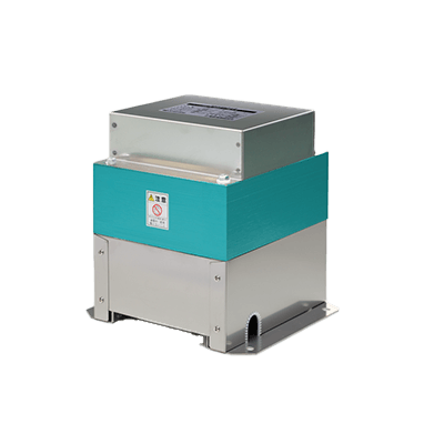
Este comienza a suministrar energía cuando la temperatura medida por el sensor de temperatura es superior a la temperatura establecida y deja de suministrar energía cuando la temperatura medida por el sensor de temperatura es inferior a la temperatura establecida.

Los sensores de temperatura permiten el funcionamiento automático de la carga en función de las condiciones de temperatura ambiente. Como resultado, el tiempo de funcionamiento de la carga se puede hacer más eficiente, lo que lleva a un ahorro de energía.

Usos de los Sensores de Temperatura

Los sensores de temperatura se utilizan para conectar cargas que funcionan con una fuente de alimentación de 100 V CA o 200 V CA y que hacen funcionar o paran la carga en función de la temperatura ambiente.

En muchos casos, los ventiladores se utilizan como cargas conectadas. Si se utiliza un ventilador como carga, el ventilador puede funcionar sólo cuando la temperatura ambiente es alta para enfriar el equipo, etc. Si se utiliza un ventilador como carga, el aire sólo podrá ventilarse cuando la temperatura ambiente sea alta.

Principio del Sensor de Temperatura

El sensores de temperatura consta de una sección de entrada de potencia, una sección de control y una sección de salida de potencia. La carga se conecta a la sección de salida de potencia y la fuente de alimentación de 100 V CA o 200 V CA para hacer funcionar la carga conectada se conecta a la sección de entrada de potencia.

1. Sección de Control

La unidad de control conecta el relé de la fuente de alimentación cuando la temperatura ambiente medida por el sensor de temperatura es superior a la ajustada, y desconecta el relé de la fuente de alimentación cuando la temperatura ambiente es ligeramente inferior a la ajustada.

2. Sección de Salida de Alimentación

La sección de salida de alimentación consta de un relé de alimentación y un fusible térmico, que suministra alimentación a la carga cuando el relé está en ON y no suministra alimentación a la carga cuando el relé está en OFF. El fusible de corriente evita que el Sensores de Temperatura se sobrecaliente, se encienda o eche humo en caso de sobrecorriente de carga.

Cómo seleccionar un Sensor de Temperatura

Los factores clave a la hora de seleccionar un sensor de temperatura son la tensión nominal y la capacidad nominal. La elección correcta ayudará a proteger contra incendios y descargas eléctricas y evitará fallos en el interruptor.

1. Tensión Nominal

Existen tres tensiones nominales para los sensores de temperatura: monofásica 100 V, monofásica 200 V y trifásica 200 V. La tensión nominal del sensor de temperatura debe ser la misma que la tensión nominal de la carga conectada.

Si se conecta una fuente de alimentación de 200 V CA a un sensor de temperatura con una tensión nominal de 100 V CA, el relé del interior del sensor de temperatura podría quemarse. Si se conecta una fuente de alimentación de 100 V CA a un interruptor de temperatura con una tensión nominal de 200 V CA, el interruptor de temperatura no funcionará correctamente debido a la insuficiente tensión de funcionamiento del relé.

2. Capacidad Nominal

La capacidad nominal de un sensores de temperatura viene definida por la corriente nominal y la corriente de arranque. La corriente asignada es la corriente en régimen permanente que circula durante el funcionamiento normal, mientras que la corriente de arranque es la corriente en régimen permanente que circula sólo cuando la carga empieza a funcionar y es un valor de corriente superior a la corriente asignada.

La capacidad nominal del sensor de temperatura debe ser superior a la capacidad nominal de la carga conectada. Si se aplica al interruptor de temperatura una corriente superior a la capacidad nominal, se fundirá el fusible de corriente del interruptor de temperatura o se fundirá el relé o se producirá un fallo de bloqueo.

Una contramedida eficaz cuando la capacidad nominal del sensor de temperatura no es suficiente es conectar un relé auxiliar, de mayor capacidad que la capacidad nominal de la carga, entre ésta y el interruptor.

3. Tipo de Adaptador

En los interruptores de temperatura generales, la conexión de alimentación donde se conectan los cables de alimentación es un bloque de terminales, mientras que en los interruptores de temperatura tipo adaptador la conexión de alimentación es una toma de corriente.

Si la conexión de alimentación es un bloque de terminales, es necesario procesar el recubrimiento del cable de alimentación antes de conectar el sensor de temperatura, mientras que con un sensor de temperatura tipo adaptador, el enchufe de alimentación de la carga conectada se puede utilizar tal cual.

Si el terminal de alimentación de la carga conectada tiene la forma de un enchufe de alimentación, es más fácil utilizar un sensor de temperatura de tipo adaptador.

カテゴリー
category_usa

Luminometer

What Is a Luminometer?

A luminometer is a type of human-detecting sensor that detects ambient light.

It has a function to automatically turn on the light when the surroundings become dark and automatically turn off the light when the surroundings become bright. It also adjusts the brightness of the display to a level that is just right for human senses. There are three main types of luminometers: phototransistors, photodiodes, and photodiodes with an amplifier circuit.

Luminometer is a technology that contributes to reducing the power consumption of electronic devices and improving the quality of display screens.

Uses of Luminometers

Luminometers are widely used to detect the brightness of displays and LCD screens and to measure ambient illuminance to automate lighting on/off.

For example, in cell phones and smartphone devices, illuminance sensors contribute to improved visibility and lower power consumption of LCD screen displays by enabling control of LCD backlight brightness in response to ambient brightness. Once mounted on a display, it can automatically adjust visibility.

It is also one of the technologies in growing demand and being adopted in a wide range of fields including cameras and optical communications.

Principle of Luminometers

Illuminometers use photodiodes and phototransistors that convert the illuminance of light incident on the light-receiving part into an electric current, which is sensed by converting the actual brightness of the light into an electrical value through a circuit that amplifies the output current to a current value usable for the sensor function.

In other words, the current flowing through the phototransistor changes according to the brightness, and this causes a voltage corresponding to the brightness to appear at both ends of the resistor installed in the circuit, thus detecting light.

In addition, the photosensitive element must have a minute sensitivity characteristic in the same range of wavelengths that can be sensed by the human eye. However, photodiodes generally used in photodetectors are sensitive outside the infrared region, which is invisible to the human eye, and thus requires compensation.

By installing a sub-photodiode with a peak spectral sensitivity in the infrared region, the sub-photodiode is subtracted from the main photodiode. This mechanism enables the sensor to have spectral response characteristics close to the visual sensitivity that the human eye can perceive.

Other Information on Luminometers

1. Output Configuration of Luminometers

There are various types of luminometers, ranging from very simple ones that convert the output current from the photodiode or phototransistor in the light-receiving part into a voltage value using an analog circuit and output it, to more sophisticated ones that have an analog-to-digital converter, a digital control unit, and a serial interface such as SPI. 

With an SPI interface, control from a microcontroller or other device is relatively easy via software and can follow the control of detailed applications. Usually, in such cases, a small dedicated IC that is converted into a sensor ASIC is used to realize a compact and highly functional luminometer product.

2. Illuminometer Sensor Switch

An applied product using luminometers is an illuminance sensor switch. Using this switch, room lighting can be automatically turned on and off according to the external brightness. For example, in a large office, there is usually a lighting switch for each area, and the lighting is turned on and off from that switch.

The advantage of installing lighting sensor switches is that lighting can be automatically turned on and off according to external brightness. Highly functional luminometer switches can also be used to dim the lights depending on the illuminance. These functions can be set from a controller installed separately from the luminometers.

From the controller, it is possible to set the level of illuminance at which the lights are turned on or off, the day of the week, and the time of day when the function is enabled. Some luminometers allow the illuminance setting to be changed depending on the season.

By installing such luminometers in offices, etc., it is possible to appropriately control the illumination level of various indoor lighting depending on the time of day, the season, and the weather conditions outside. Such efforts will result in energy savings.

カテゴリー
category_es

Medidores de Campo Electromagnético

¿Qué es un Medidor de Campo Electromagnético?

Un medidor de campo electromagnético es un instrumento utilizado para medir la intensidad de los campos eléctricos.

Se utiliza principalmente para medir la intensidad de las ondas de radio recibidas por radios y televisores, y las ondas de radio generadas por equipos electrónicos. En los últimos años, se han empezado a utilizar muchos dispositivos electrónicos que emiten ondas de radio.

A medida que aumenta el riesgo de interferencias de radio entre los dispositivos electrónicos y el efecto de las ondas de radio en el cuerpo humano, hay una gran necesidad de medidores de campo electromagnético que puedan medir con precisión la intensidad de campo.

Usos de los Medidores de Campo Electromagnético

Dado que los medidores de campo electromagnético pueden medir la intensidad de las ondas de radio, se utilizan para investigar la ubicación de la instalación de equipos que reciben ondas de radio y para inspeccionar la seguridad de los equipos que emiten ondas de radio.

En las inspecciones de la ubicación de instalación de equipos que reciben ondas de radio, son útiles en las inspecciones para la instalación de antenas para la recepción de emisiones de TV, y en las inspecciones en las que hay interferencias con la recepción de emisiones de TV. Recientemente, ha aumentado la medición de la intensidad de las ondas de radio WiFi.

Se utilizan en inspecciones de seguridad de equipos que emiten ondas de radio para reducir el riesgo de interferencias de equipos que generan ondas de radio y el riesgo de las directrices de defensa de la bioseguridad de los campos electromagnéticos y los efectos de las ondas de radio en el cuerpo humano.

Principio de los Medidores de Campo Electromagnético

El método más común para medir la intensidad de las ondas de radio consiste en medir la tensión inducida en una antena de ganancia conocida con un medidores de campo electromagnético. El valor medido se convierte a una antena con una longitud efectiva de 1 m y se expresa en unidades [dBμV/m].

1. Intensidad de Campo Radioeléctrico en el Espacio

Existen diferentes métodos de medición para los medidores de campo electromagnético, dependiendo de la aplicación. Para medir simplemente la intensidad de las ondas radioeléctricas en el espacio, se apunta una sonda de campo hacia el dispositivo sometido a prueba. La sonda de campo suele utilizar un modulador EO (modulador electro-óptico) para detectar la intensidad de las ondas de radio.

En ausencia de campo eléctrico, la luz procedente de una fuente luminosa de la sonda de campo atraviesa una fibra óptica y se refleja en un cristal EO. A continuación, pasa por otra fibra óptica y se emite.

En presencia de una carga eléctrica, el cristal EO modifica el índice de refracción de la luz, de modo que la luz de salida tiene un índice de refracción diferente al de la luz de entrada. Al convertir la luz modulada en información de intensidad mediante un fotodetector, los medidores de campo electromagnético miden la intensidad del campo eléctrico.

2. Absorción de Ondas de Radio en el Cuerpo Humano

Para investigar, por ejemplo, la eficacia de absorción de las ondas de radio en el cuerpo humano, debe intercalarse un dispositivo denominado “maniquí” entre el dispositivo sometido a prueba y la sonda de campo eléctrico.

El maniquí tiene características eléctricas iguales a las del cuerpo humano. La sonda de campo de un medidor de campo electromagnético consiste en una fibra óptica, un cristal EO y un tubo de vidrio que lo cubre; el cristal EO tiene un efecto EO, en el que el índice de refracción de la luz cambia dependiendo del campo eléctrico presente, y la señal moduladora es detectada por un fotodetector.

Más Información sobre Medidores de Campo Electromagnético

1. Medidores de Campo Electromagnético en Kit

La principal diferencia entre los medidores de campo electromagnético de kits de montaje baratos disponibles en el mercado y los vendidos por los fabricantes es la diferencia significativa en el rendimiento, la comodidad y la versatilidad. Por ejemplo, en los kits económicos, la pantalla es un medidor de aguja analógico.

En cambio, los medidores de campo electromagnético de los fabricantes tienen una pantalla LCD en color, pueden almacenar los datos obtenidos en la memoria y pueden conectarse a otros dispositivos mediante comunicación. Por lo tanto, se puede decir que los Medidores de Campo Electromagnético son más para uso educativo o temporal.

2. Apps de Medidores de Campo Electromagnético 

Recientemente, la intensidad de las señales WiFi puede medirse mediante medidores de campo electromagnéticos. Sin embargo, se requiere cierto cuidado en su configuración. Cuando se configura una red inalámbrica, la cobertura apenas cambia.

La señal se debilita cuando atraviesa muebles o paredes, por ejemplo. Lo mismo ocurre con las interferencias causadas por otras redes inalámbricas cercanas: el WiFi se debilita progresivamente a medida que uno se aleja del router de origen.

Si los usuarios reciben una señal fuerte, pueden conseguir cargas rápidas de páginas y descargas instantáneas. Para que el router envíe una señal potente allí donde se necesita, es importante elegir la ubicación y la configuración adecuadas del router para obtener los mejores resultados.

Recientemente, existen aplicaciones que muestran un mapa visual del alcance inalámbrico del router y muestran información sobre otras redes WiFi y la intensidad de campo de la señal WiFi. Estas aplicaciones visualizan la intensidad de la señal de la red inalámbrica en forma de un práctico mapa de calor para ayudarte a decidir dónde colocar el router.

カテゴリー
category_usa

Isolation Transformer

What Are Noise Cut Transformers?

Noise Cut TransformerA noise-cut transformer is a device designed to prevent noise interference. It is a trademark developed by DENKEN SEIKI KOGYO K.K. in 1960 and is also called Isolation Transformers, although its common names are fault wave isolation transformers and transformers for noise suppression. Noise-cut transformers are a practical application of transformer-type noise prevention elements.

Since it separates and isolates the source of the noise and the electric circuit on the side disturbed by the noise, it is highly effective in preventing noise. Also, because it is a separate isolation type, it can function even in a poor electromagnetic environment.

Uses of Noise Cut Transformers

Many modern devices are high-speed and multifunctional, which makes our lives more convenient. Since these devices are operated by micro-voltages, they may malfunction due to noise entering from the outside.

Lightning, amateur radio, automobiles, discharge equipment, home appliances, and medical equipment are all subject to external noise intrusion. Noise Cut Transformers can prevent these noises, and the noise itself that they emit will not leak into external circuits.

Principle of Noise Cut Transformers

Noise Cut Transformers prevent noise from entering the secondary side. There are two types of noise: common mode and normal mode.

1. Common Mode

In the case of common mode noise, low-frequency noise (around several 10 kHz) can be somewhat attenuated by Noise cut transformers. However, as the noise frequency increases, noise penetration into the secondary side increases due to the capacitance between the primary and secondary sides of the transformer.

In this case, noise-cut transformers can prevent noise intrusion by adding an electrostatic shield between the primary and secondary coils and grounding it.

2. Normal Mode

Normal mode noise is output on the secondary side as it is, so the transformer itself has no suppression effect. For example, the frequency of noise caused by lightning is very high compared to the frequency of power supplies for general equipment (50/60 Hz).

By taking advantage of this, noise in the normal mode can be suppressed by having the filter pass through the lower frequencies of the power supply and weaken the higher frequencies.

Structure of Noise Cut Transformers

In addition to the structure of conventional isolation transformers, the structure of noise-cut transformers consists of multiple encircling electromagnetic shielding plates around the periphery of the coil transformer. In addition, the coil arrangement, core material, and shape are designed so that the magnetic flux of high-frequency noise does not interlock with each other. This prevents the transmission of noise due to capacitive coupling and electromagnetic induction.

When noise is to be cut, the usual measure is to isolate the source of the noise. The actual isolation measure is almost always a photocoupler on the circuit. If a photocoupler is not used, the method of dealing with the problem is a noise-cut transformer.

For cost and space reasons, it is preferable to use a photocoupler on the circuit board, but if a circuit board is not available, a noise-cut transformer is used. However, noise-cut transformers are not a panacea, and the secondary winding is also affected by noise from the primary winding. The use of noise-cut transformers can solve this problem.

Other Information on Noise Cut Transformers

Grounding of Noise Cut Transformers

Some measures can be taken to prevent noise, even in locations with different potentials between the ground of an electrical circuit and the earth, or in cases where grounding is not possible. One such measure is to install noise-cut transformers.

If this is still ineffective, ensure that the area where noise-cut transformers are installed makes contact with the ground over as large an area as possible. Another effective method is to make the input and output cables into shielded wires that can shield noise, and install this shielded wire and the case of noise-cut transformers over a large area. This is expected to improve the noise rejection effect.

カテゴリー
category_usa

FPD Lithography Equipment

What Is FPD Lithography Equipment?

FPD (Flat Panel Display) lithography equipment exposes light to a photomask, which is an original plate with a circuit pattern of a thin-film transistor (TFT) to be formed on a glass substrate for manufacturing LCDs and organic EL displays. The FPD exposure system exposes the TFT circuit pattern on the photoresist coated on the glass substrate.

The technology of FPD lithography equipment is based on the photolithography technology used in semiconductor manufacturing. However, unlike the exposure technology used in semiconductor manufacturing, new technology, such as repeated multiple exposures, is required for FPDs, because one side of a semiconductor chip is approximately 1 cm in size, whereas the size of an FPD can reach several meters.

In addition, the number of TFT circuits must be increased according to the number of pixels to achieve higher resolution. For example, a 4K LCD with more than 8 million pixels requires the formation of more than 24 million TFT circuits (8 million x RGB (red, green, and blue) color filters), and an OLED requires the formation of several times as many TFT circuits.

Uses of FPD Lithography Equipment

FPD lithography equipment is used to manufacture various types of FPDs. Currently, liquid crystal displays (LCDs) are the most common type of FPDs, and they are used in a wide range of monitors, from mobile devices such as smartphones to information processing. Other applications include vehicle, aircraft, and medical applications.

In addition to LCDs, there are various other types of FPDs such as PDPs, organic ELs, inorganic ELs, and VFDs (fluorescent display tubes).

The mechanism common to these various types of FPDs is the function of controlling each pixel to display an image as a whole, and the role of FPD lithography equipment is to form the TFTs that control this function using exposure technology.

Principle of FPD Lithography Equipment

FPD lithography equipment consists of a light source, an optical system including lenses, and a stage on which a substrate is mounted.

Ultraviolet rays from super high-pressure mercury lamps are mainly used as the light source, but as TFT circuits become finer, the wavelength of ultraviolet rays becomes shorter.

The optical system controls the position and focus of the photomask and lens. Since nm-order TFT circuits must be formed precisely for higher resolution, the system not only irradiates light with high precision but also measures the distortion and position of the photomask and mother glass surface. In addition, it corrects them by controlling the optical system and stage.

Types of FPD Lithography Equipment

Stepper and Scanner Systems

There are two main types of FPD lithography equipment: stepper systems and scanner systems.

In the stepper method, the entire surface of the photomask is irradiated at once to expose the target glass substrate, and then the process moves on to the next glass substrate. It can process a single glass substrate or multiple glass substrates such as 2 x 2 at a time. However, one disadvantage is that it is difficult to make larger sizes and the overall resolution is low because the focus is on the center of the mask. For this reason, it is used for small LCDs, etc. However, one of the advantages is that equipment is inexpensive.

In the scanner method, the light source is narrowed down and irradiated to a portion of the photomask, and the entire surface of the photomask is exposed while scanning the irradiated position. While this has the advantage of enabling the manufacture of large glass substrates and increasing resolution by using only the light from the center of the mask, it has the disadvantage of requiring time to scan the entire surface and increasing equipment costs.

Currently, the scanner method is the mainstream due to the demand for larger sizes and higher resolution.

Other Technologies

Multi-lens method is a technology that supports larger substrates. This technology expands the exposure area by using multiple lenses in a row, and it applies to both steppers and scanners.

Conventional exposure technology using photomasks is suitable for mass production, but the cost and time required to create photomasks are disadvantages for prototyping and low-volume, high-mix production. For this reason, maskless exposure technologies that do not use photomasks are being developed. This technology uses a DMD (Digital Micromirror Device) made with MEMS (Micro Electromechanical System) technology to irradiate substrates by switching several hundred thousand beams individually at ultra-high speed. This reduces the time and cost of prototyping and low-volume, high-mix production.

カテゴリー
category_de

Holzhammer

Was ist ein Holzhammer?

Ein Holzhammer ist aus Holz gefertigt und im Gegensatz zu Metallhämmern sehr leicht. Da er aus Holz besteht, ist es auch unwahrscheinlich, dass er die Person, auf die er schlägt, verletzt.

Er ist sehr nützlich, wenn es darum geht, Hämmer für feine Positionsanpassungen leicht zu klopfen. Kleinere Größen können mit einer Hand bedient werden, aber einige größere sind so schwer, dass sie nur mit beiden Händen gehalten werden können. Wenn Sie einem Gegenstand einen großen Schlag versetzen wollen, müssen Sie mit schweren Gegenständen hantieren.

Anwendungen von Holzhammern

Die grundlegende Verwendung ist die gleiche wie bei einem gewöhnlichen Hammer. Schlagen Sie mit dem Hammer auf den Gegenstand, auf den Sie schlagen wollen. Das Risiko, den Gegenstand zu zerkratzen, ist gering, aber die Schlagkraft ist ausreichend. Wenn der Hammer Ihre Hand trifft, können Sie sich ernsthaft verletzen.

Behalten Sie beim Schlagen den Hammer im Auge und zielen Sie genau. Auch wenn das Objekt nicht leicht verkratzt werden kann, ist es doch wahrscheinlicher, dass es verformt oder zerkratzt wird, wenn das Objekt weich ist. Beim Hämmern ist es wichtig, sich zu überlegen, wie viel Kraft man aufwenden muss.

Auswahl eines Holzhammers

Es gibt nur wenige verschiedene Arten von Holzhammern, aber hier sind einige Unterschiede zwischen ihnen:

  • Kopfform
    Die meisten Holzhammer haben einen zylindrischen Kopf. Es gibt jedoch auch Hammer mit einem quadratischen Prisma.
  • Hammer mit Eisenkern
    Diese Art von Hammer hat einen Eisenkern im Inneren des Hammerkopfes. Die Größe des Hammers ist gleich, aber das Gewicht wird durch den Stahlanteil erhöht, so dass der Hammer eine größere Schlagkraft entwickeln kann. Geeignet für die Verformung von Gegenständen, ohne sie zu beschädigen, und für den Abbruch von Holz.
  • Mit Stahlplatte
    Dieser Hammer hat eine Eisenplatte, die an einer Seite des Kopfes angebracht ist. Er ist ein nützlicher Hammer, der sowohl die Funktionen eines Holzhammers als auch die eines Eisenhammers erfüllt. Neben Abbrucharbeiten kann die Eisenplatte auch zum Einschlagen von Nägeln und Pfählen verwendet werden.
  • Kleiner Arbeitshammer
    Dieser Hammer ist mit einem kleinen Kopf ausgestattet. Wie der Name schon sagt, ist er für Detailarbeiten geeignet. Wenn er klein ist, kann er für Abbrucharbeiten verwendet werden, aber er bietet keine große Schlagkraft.
カテゴリー
category_de

Bolzenschneider

Was ist ein Bolzenschneider?

Bolzenchneider sind Werkzeuge zum Schneiden von weichen Kupferdrahtmaterialien wie Eisendraht, verzinktem Eisen und Litzendraht.

Beim Schneiden gehen die Klingen nicht wie bei einer Schere übereinander, sondern greifen in den Draht und quetschen ihn beim Schneiden. Bolzenschneider und Litzenschneider sind ähnliche Werkzeuge.

Zwergenzangen ähneln baugleich Bolzenschneidern, haben aber eine höhere Schneidkapazität. Der abgewinkelte Klingenabschnitt ermöglicht das Schneiden von der Basis des Drahtmaterials her. Schnurschneider haben ebenfalls den gleichen Grundaufbau wie Bolzenschneider, aber die Schneide hat eine spezielle Form, die zum Schneiden von Kabeldrähten und Drahtseilen geeignet ist.

So verwenden Sie Bolzenschneider

Legen Sie das zu schneidende weiche Kupferdrahtmaterial zwischen die Klingen des Bolzenschneiders in der Mitte der Klinge und fixieren Sie es dort.

Die Klinge wird dann durch Ergreifen des Griffs mit der Hand geschlossen. Wenn Sie dickeres Weichkupferdrahtmaterial schneiden wollen, ist es einfacher, das Drahtmaterial so weit wie möglich von der Klinge entfernt zu halten und zu fixieren.

Wenn beim Befestigen des zu schneidenden weichen Kupferdrahtes an der Klinge ein großer Spalt entsteht und der Draht nicht abgeschnitten werden kann, lösen Sie die Einstellmutter und stellen Sie die Höhe des Einstellbolzens auf die entsprechende Position ein, während Sie die Öffnung der Klingenspitze überprüfen. Dadurch wird der Spalt zwischen Walzdraht und Klinge beseitigt und ein reibungsloses Schneiden ermöglicht.

Auswahl eines Bolzenschneiders

Achten Sie bei der Auswahl eines Bolzenschneiders immer auf die maximale Schneidkapazität und die zu schneidenden Materialien. Wählen Sie außerdem einen Bolzenschneider, dessen Klingenmaterial, Konstruktion und Funktionsweise für die Umgebung und den Verwendungszweck geeignet sind. Im Folgenden finden Sie eine Zusammenfassung der Punkte, die bei der Auswahl eines Bolzenschneiders zu beachten sind:

  • Material des Klingenteils
    Bolzenschneider mit Klingenteilen aus rostfreiem Stahl sind rostbeständig und ziehen beim Schneiden von rostigem Draht keinen Rost an, sodass sie sich für den Einsatz im Freien bei nassem Wetter oder an Orten, an denen sie nass werden können, eignen. Rost an den Klingenteilen kann auch dadurch verhindert werden, dass man sie nach dem Gebrauch einfach mit Wasser abwäscht.

Bolzenschneider mit Kupferklingen haben eine hervorragende Schärfe und Haltbarkeit, sodass sie wie eine Schere mit einer Hand am Griff bedient werden können, um Walzdraht schnell und mit geringem Kraftaufwand zu schneiden.

  • Funktionsweise
    Bei Arbeiten in der Höhe sind Bolzenschneider nützlich, die so beschaffen sind, dass sie an einem Karabinerhaken am Hüftgurt befestigt werden können und über eine Öffnung zur Befestigung eines Sicherungsseils verfügen, um einen Absturz zu verhindern. Wenn der Bolzenschneider nicht für die Befestigung an einem Karabiner vorgesehen ist, kann ein separater Werkzeughalter für den Bolzenschneider verwendet werden, um ihn am Hüftgurt zu befestigen.