What Is a Phototransistor?
 A phototransistor is a semiconductor device used to detect light.
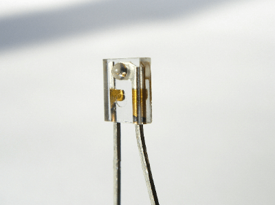
Its structure is a combination of a phototransistor and a photodiode. Since they are available in a variety of shapes depending on the package, they must be selected appropriately for each application.
Uses of Phototransistors
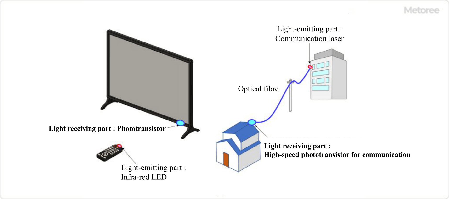
Figure 1. Uses of phototransistors
Phototransistors are widely used as light-receiving sensors. In particular, since they have a peak sensitivity around 800 nm, they are generally used to receive infrared light.
Specific examples of phototransistor applications include “light intensity measurement,” “infrared remote control receivers,” “photoelectric sensor receivers,” and “optical communications.” In particular, they are often used in combination with infrared LEDs in remote controls for TVs and air conditioners.
One application of optical communication is the gigabit optical communication service provided by internet providers. The light receiving part of that communication uses high-speed phototransistors, which are ideal for communication.
Phototransistors are also sometimes used as sensors in automatic doors. Furthermore, since phototransistors generate electric current by detecting light, they are used as switches driven by light, and so on.
Structure of Phototransistors
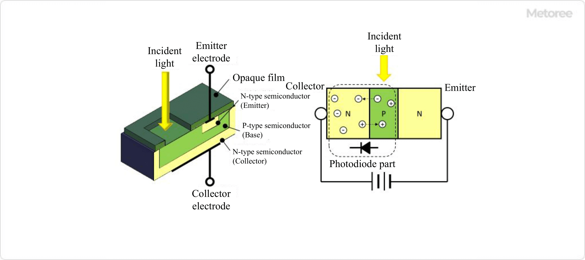
Figure 2. Structure of phototransistor
Phototransistors are semiconductor devices with an NPN structure. This NPN structure allows the phototransistor to produce a larger output signal than a photodiode.
The NPN structure of the phototransistor amplifies the output of the photodiode with a transistor. When light equivalent to the energy gap of the semiconductor enters the transistor, electrons in the valence band are excited to the conduction band.
This causes migration to the N layer, and holes move to the P layer. This transfer from the N layer to the P layer causes a forward bias at the junction, which results in a current flow.
The transistor used in phototransistor is characterized by the fact that it does not have a base electrode. However, the photocurrent generated by light reception becomes the base current, and this base current is amplified by the collector.
Features of Phototransistors
The amplification of the base current is hFE (transistor amplification factor) times as large as that of other transistors. However, as a characteristic of phototransistors, even if the hFE is the same, there is a tendency to use a relatively large hFE.
This allows a large collector current to be drawn from the tiny photodiode signal, but it should be noted that current is always leaking at the collector-base junction, and this leakage current is also amplified.
In other words, phototransistors have a weak current flow even in a completely dark environment. This weak current that flows even in a dark environment is called dark current. The dark current generated by a phototransistor is an internal noise as a light sensor. However, it is possible to suppress this internal noise.
The dark current has the characteristic of increasing when the temperature is high and, conversely, decreasing when the temperature is low. Therefore, internal noise can be suppressed by cooling the device using this characteristic.
Other Information on Phototransistors
1. Phototransistor and Transistor
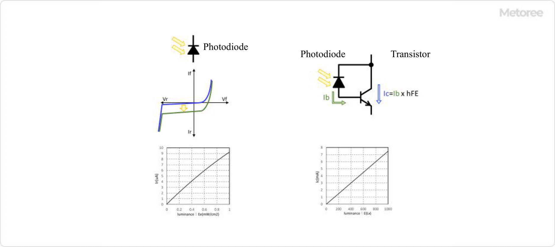
Figure 3. Photodiode and transistor
The IV characteristic of a photodiode shifts downward in response to the intensity of light (blue line becomes green line) when it is exposed to light. This change in IV characteristic is the standard for measuring light intensity. However, since the output current is in the order of uA, the output as it is would complicate the circuitry in the subsequent stages.
By combining a phototransistor with a photodiode and a transistor, it is possible to amplify the photocurrent generated when light is received by the photodiode by a factor of hFE, the DC current amplification factor of the transistor. Therefore, the phototransistor is more sensitive than the photodiode, and the output current of the phototransistor is in the order of mA, thus simplifying the circuitry in the subsequent stages.
Phototransistors are several hundred times more sensitive than photodiodes, and if even higher sensitivity is required, the use of a Darlington-connected phototransistor can provide several hundred times x several hundred times higher sensitivity. This makes it possible to detect brightness of several Lux.
2. Difference Between a CDS and Phototransistors
A CDS is a photoresistor, also called a CDS cell or a photoconductive cell. That is, the resistance increases when the illuminance is low and decreases when the illuminance is high.
The advantages of CDS are that the minute sensitivity characteristic is close to that of human vision. The structure is simple; the sensitivity is high, and the price is low.
For example, they are used in illuminance meters, exposure meters for cameras, and brightness detectors for automatic flashing lights. However, cadmium sulfide, the main material used as an element in CDS, is an environmentally harmful substance. For this reason, the use of CDS has been decreasing in recent years.
Phototransistors, on the other hand, provide an output current proportional to illuminance. Another advantage of phototransistors is their high sensitivity because of their structure, which combines a photodiode and a transistor.